Service hotline
+86 0755-23615795

Release date:2025-07-23Author source:KinghelmViews:8
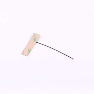
In wireless communication systems, the PCB antenna, as a key component for transmitting and receiving signals, directly affects communication quality. Achieving 50-ohm impedance matching is critical for ensuring efficient signal transmission. If impedance is mismatched, it leads to signal reflection, increased loss, and significantly reduced transmission efficiency. This article will deeply analyze the principles, design methods, optimization strategies, and common troubleshooting techniques for 50-ohm impedance matching in PCB antennas, helping you master this essential technology.
Impedance represents the resistance to current in a circuit, including contributions from resistance, inductance, and capacitance. In PCB antenna systems, the antenna’s impedance must match the impedance of the RF front-end circuit, typically set at 50 ohms, to achieve maximum power transfer and minimize signal reflection. Simply put, impedance matching is like aligning the diameter of two connected pipes—only when the diameters are equal can water (the signal) flow smoothly; otherwise, backflow occurs, wasting energy.
When the PCB antenna’s impedance doesn’t match 50 ohms, part of the signal reflects back to the transmitter, forming standing waves. The Voltage Standing Wave Ratio (VSWR) measures the degree of impedance matching; the closer the VSWR is to 1, the better the matching. When VSWR exceeds 2, signal loss increases significantly. For instance, at a VSWR of 3, about 25% of signal energy is reflected, which severely affects antenna performance.
1. Adjusting Antenna Dimensions:
By modifying the length, width, and bend angles of a PCB antenna, its impedance can be tuned. For example, in an inverted-F antenna, shortening the arm length decreases impedance, while increasing it raises impedance. Designers usually use professional simulation tools (like ADS or HFSS) to create 3D models, simulate impedance changes for different dimensions, and iteratively optimize toward 50 ohms.
2. Changing Feed Point Location:
The feed point location greatly affects antenna impedance. Moving the feed point toward the antenna’s end increases impedance; moving it closer to ground decreases impedance. In practice, designers often test multiple feed points along the antenna to identify the location where impedance is closest to 50 ohms.
1. Pi (π) Matching Network:
Consists of two capacitors and one inductor arranged in the shape of the Greek letter π. By selecting suitable capacitor and inductor values, antenna impedance can be effectively adjusted. For example, in a 2.4 GHz PCB antenna, a π network using a 1.8 nH inductor and two 15 pF capacitors can match an antenna impedance of 75 ohms down to 50 ohms.
2. T Matching Network:
Composed of two inductors and one capacitor, suitable for scenarios with larger impedance differences. During design, the specific inductor and capacitor values are calculated based on the initial and target impedances, either through formulas or using Smith charts as a design aid.
1. ADS (Advanced Design System):
A powerful EDA tool for modeling and simulating PCB antennas. In ADS, you can input antenna dimensions and material properties, then use harmonic balance, method of moments, and other algorithms to quickly calculate antenna impedance and VSWR, and receive optimization suggestions.
2. HFSS (High Frequency Structure Simulator):
Based on finite element analysis, HFSS can accurately simulate the antenna’s electromagnetic characteristics in 3D space. Using HFSS, designers can visually observe impedance distribution and electric/magnetic field strength, helping to refine antenna structures and matching network designs.
1. Minimizing Interference:
Keep the antenna sufficiently far from power modules and digital circuits on the PCB—ideally at least 10 mm. Also, avoid running high-speed signal traces near the antenna to prevent electromagnetic interference that could affect impedance.
2. Improving Ground Design:
Good grounding is critical for impedance matching. Design an independent ground plane for the antenna, add more ground vias, and ensure the ground paths are short and wide. Large copper pours can be used as ground layers to reduce ground impedance and minimize signal reflection.
1. Dielectric Substrate:
The dielectric constant and loss tangent of the substrate significantly influence antenna impedance. Choose stable, low-loss materials like the Rogers series. For example, Rogers 4350B has a dielectric constant of 3.48 and a loss tangent of only 0.0037, which helps achieve precise impedance matching.
2. Metal Traces:
Trace width and copper thickness also impact impedance. Increasing copper thickness reduces resistance and signal loss; adjusting trace width fine-tunes impedance. Generally, wider traces reduce impedance, while narrower traces increase it.
If measured VSWR exceeds 2, first check if the antenna structure matches the design and whether there are manufacturing errors. If the structure is correct, try tuning the matching network parameters, or add adjustable capacitors/inductors for on-the-fly tuning. Also, verify that the PCB grounding is reliable, checking for cold solder joints or shorts.
If antenna impedance deviates from 50 ohms, minor deviations can be corrected by adjusting the matching network. For larger deviations, revisit the antenna design—adjust dimensions or feed point location. Also confirm the accuracy of material parameters, as variations between material batches can affect impedance.
Some PCB antennas experience impedance drift with temperature changes. Consider using materials with low temperature coefficients, like ceramic substrates. Additionally, design temperature compensation circuits with thermistors or variable capacitors to automatically adjust the matching network and offset temperature effects.
Designing a 50-ohm impedance match for PCB antennas is a comprehensive task that requires understanding theory, mastering design methods, applying optimization strategies, and troubleshooting real-world issues. By adjusting antenna structure, adding matching networks, optimizing PCB layout, choosing suitable materials, and leveraging professional simulation tools, designers can achieve efficient impedance matching and enhance PCB antenna signal performance.
Copyright © Shenzhen Kinghelm Electronics Co., Ltd. all rights reservedYue ICP Bei No. 17113853