Service hotline
+86 0755-23615795

Release date:2025-07-16Author source:KinghelmViews:53
As a core wireless component in compact electronic devices—such as smartwatches, Bluetooth earphones, and IoT sensors—Bluetooth patch antennas are widely used for their small size (typically 5–20 mm) and high level of integration. However, during installation and debugging, many engineers wonder: Does a Bluetooth patch antenna have positive and negative terminals? Will reversing the connection affect performance?
This article answers these questions in detail by exploring the structural design, electrical characteristics, and installation standards, helping you avoid performance issues caused by wiring mistakes.
1. Structure of a Bluetooth Patch Antenna: No “Positive/Negative” but a Defined “Feed Point”
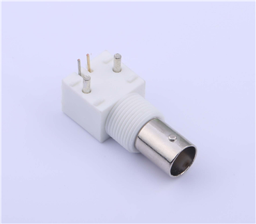
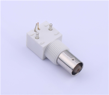
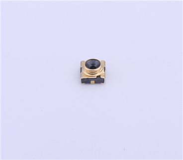
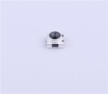
(1) Key structural components
Bluetooth patch antennas (typically operating in the 2.4–2.485 GHz band) usually consist of:
l Radiating patch: A metal conductor (copper or silver paste) printed on the PCB, responsible for transmitting and receiving electromagnetic waves.
l Ground plane: A large metal layer under the patch (usually part of the device’s motherboard), which serves as the signal reference ground and affects impedance matching and radiation pattern.
l Feed point: The RF signal interface connecting the patch to the RF chip via a microstrip line.
(2) The misconception of “positive and negative”
In DC circuits, “positive and negative” refer to power supply polarity (e.g., battery terminals).
However, Bluetooth patch antennas operate with RF AC signals (2.4 GHz, oscillating 2.4 billion times per second), so there is no DC positive/negative.
What really matters is correct connection of the feed point and ground plane—not polarity.
2. Importance of the Feed Point and Ground: Wrong Connections Can Disable the Signal
The performance of a Bluetooth patch antenna depends on proper electrical connection between the feed point and ground plane. Incorrect connections can cause serious issues:
(1) Correct connection
l The feed point should connect to the RF output of the Bluetooth chip (e.g., RF_OUT pin) through a 50 Ω microstrip line.
l The ground plane should be reliably connected to the system ground (GND) of the motherboard (usually via vias or conductive adhesive) to complete the RF circuit.
This ensures efficient RF transmission to the radiating patch, achieving a typical VSWR < 1.5, low reflection, and radiation efficiency > 70%.
(2) Consequences of wrong connections
l Feed point reversed: Connecting the feed point to ground shorts the RF signal directly to GND, resulting in no output. Reception sensitivity can drop by over 30 dB, effectively weakening the signal by a factor of 1000.
l Poor grounding: If the ground plane isn’t properly connected to system ground (e.g., due to cold solder joints or oxidized vias), impedance mismatch (VSWR > 3) can occur, causing severe signal reflection and reducing range from ~10 m to 1–2 m.

(1) Check the datasheet
Reputable Bluetooth patch antennas include a datasheet clearly labeling:
l The feed point (often marked as “RF IN,” “Feed,” or with a dot “●”)
l Ground areas (marked as “GND” or shaded regions)
For example:
l Some antennas have “Pin 1 = Feed; Pins 2–4 = Ground”
l FPC (flexible) antennas usually have silk screen labels “RF” and “GND”
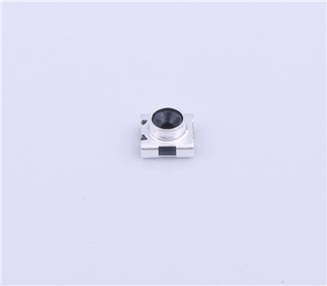
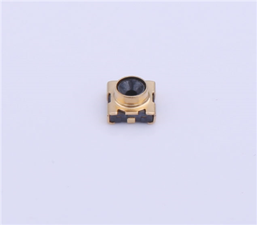
(2) Observe the physical structure
l The feed point is typically a small solder pad (diameter ~0.5–1 mm) directly connected to the radiating patch.
l The ground plane is a large metal area (covering > 60% of the antenna) with visible insulation gaps (typically 0.1–0.3 mm) separating it from the patch.
(3) Use a multimeter (with power off)
l The feed point and ground plane should show infinite resistance (they’re isolated).
l The ground plane and edge ground pads should show ~0 Ω (conductive, part of GND).
Even after identifying the feed and ground, details matter for performance:
(1) Avoid long or sharply bent feed lines
The microstrip from the feed point to the chip should be < 30 mm and as straight as possible (avoid 90° bends). Extra length adds loss (~0.2 dB per 10 mm). For instance, a 20 mm feed line performs ~0.6 dB better than a 50 mm line, which can extend range by ~15%.
(2) Keep the ground plane “clean”
Do not place metal parts (screws, shields) or high-frequency signal lines (e.g., clock lines) over the ground plane. This can block or distort the antenna’s pattern (main lobe shift > 10°).
(3) Follow proper soldering practices
l Soldering temperature: 260 ± 10 °C, duration < 3 s to avoid damaging the patch.
l Proper solder volume: pad height ~0.3–0.5 mm. Too much can short the feed to ground; too little can cause poor contact.
Q1: Does a Bluetooth patch antenna have positive/negative markings?
A: No true “positive/negative.” But quality products label the feed point (“RF”) and ground (“GND”). Follow these labels when connecting.
Q2: Will reversing the connection render it useless?
A: In most cases, yes. In rare cases where the feed and ground are very close (< 0.5 mm), you might get a weak signal, but range drops to ~1/10 of normal.
Q3: Are there special installation requirements for flexible (FPC) Bluetooth patch antennas?
A: Yes. The ground side should be glued to the device’s ground with conductive adhesive (contact resistance < 0.1 Ω). Avoid folding or stretching, as this changes the patch dimensions and can shift the frequency ±50 MHz.
Bluetooth patch antennas do not have DC “positive and negative” terminals. Instead, proper connection of the feed point to the RF signal and the ground plane to system GND is critical.
Always follow the datasheet, ensure reliable ground connections, and avoid poor soldering or metallic obstructions.
Mastering these details helps prevent issues like weak signal or limited range, ensuring stable wireless communication for your Bluetooth devices (e.g., fitness trackers, wireless earbuds).
If you encounter abnormal signal performance during assembly, check the feed and ground connections first—this often quickly reveals the root cause.