Service hotline
+86 0755-23615795
Release date:2025-08-07Author source:KinghelmViews:172
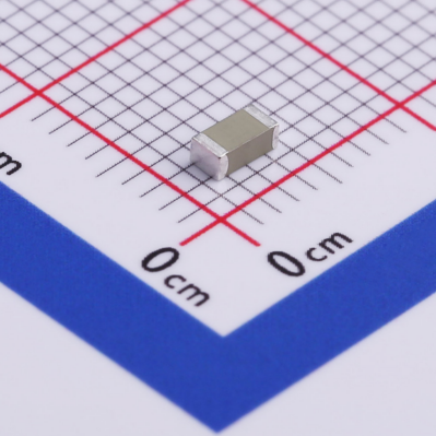
With ultra-compact dimensions (as small as 2mm × 3mm) and high frequency stability (within ±5MHz), Bluetooth ceramic chip antennas have become core wireless components in miniature electronic devices such as wearables and medical equipment. Their ability to maintain stable communication over 10 meters in a space no larger than a fingernail is made possible by their precisely engineered multilayer structure. This article systematically dissects the internal structure of Bluetooth ceramic chip antennas, highlights the material characteristics, explains the structural-performance relationships, and analyzes common structural defects—helping engineers and procurement professionals understand how these antennas work and avoid selection and application pitfalls.
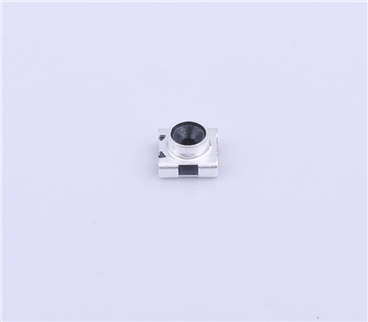
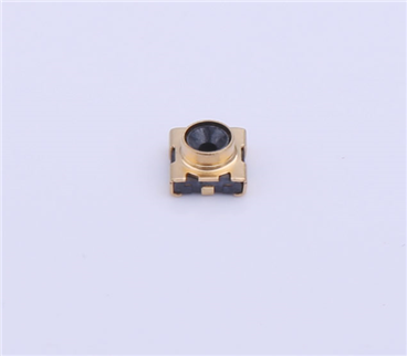
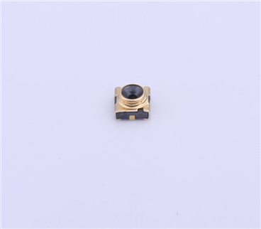
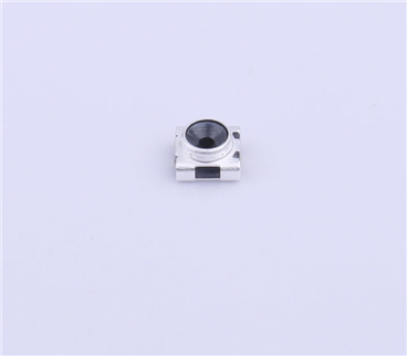
I. The 4-Layer Core Structure of a Bluetooth Ceramic Chip Antenna (Function Breakdown from Inside Out)
The performance of Bluetooth ceramic chip antennas is defined by a laminated structure, where each layer's material, dimension, and processing precision directly affect radiation efficiency. Even a 0.05mm deviation may result in a 30% drop in performance.
Core Function: Acts as the physical support for the antenna while compressing the electromagnetic wavelength through a high dielectric constant (εr), enabling efficient radiation in a compact form.
Common Materials & Parameters:
90% Alumina (Al₂O₃): εr = 10–15, suitable for devices with moderate size sensitivity (e.g., Bluetooth earbuds).
96% Alumina: εr = 20–30, can shrink the antenna size to 1/4 of an FR4-based antenna (e.g., in 2.4GHz applications, edge length only ~3mm); widely used in smartwatches.
Barium Titanate (BaTiO₃): εr = 50–90, enables the smallest sizes (down to 2mm × 2mm), but exhibits high temperature coefficient of frequency (±10ppm/°C), requiring compensation circuits.
Structural Details: Thickness ranges from 0.5–1.5mm (typically 1mm); surface flatness should reach Ra ≤ 0.1μm to ensure firm adhesion with the metal layer and avoid poor contact.
Core Function: Converts RF current from the Bluetooth module into a 2.4GHz electromagnetic wave, serving as the signal outlet.
Material & Process:
Made from oxygen-free copper foil (99.9% purity), applied via thick-film printing (precision ±0.03mm) or sputtering. Thickness: 3–5μm (too thin = prone to oxidation; too thick = impairs high-frequency performance).
Common shapes: rectangular (for omnidirectional radiation, e.g., smart home devices) or inverted-F (PIFA) (uses a shorting stub for impedance tuning, with matching accuracy up to 50Ω ±3Ω; suitable for metallic environments like smartwatches).
Key Parameter: Length must precisely match 1/4 wavelength of 2.4GHz signal, compressed by εr. Formula: λ = 31mm / √εr. For εr = 25, length = 6.2mm.
Core Function: Reflects downward electromagnetic waves into open space (reducing internal absorption) and provides a stable ground reference, minimizing impedance fluctuations.
Structural Requirements:
Area ≥ 2× that of the radiating element (e.g., 3mm × 3mm radiator → ≥6mm × 6mm ground); same copper material as radiator.
Connected to the device’s PCB ground via 1–2 ground vias (diameter: 0.3–0.5mm); ground resistance should be <0.05Ω (every 0.1Ω increase reduces efficiency by 5%).
Design Pitfall: Insufficient ground plane area can cause signal "leakage" into the device, shortening transmission range by over 40%. Proper area ratio is critical.
Core Function: Prevents radiator oxidation (copper oxidizes within 3 months in open air, shifting impedance) and blocks moisture ingress (humidity >80% shortens lifespan to ~1 year without protection).
Common Materials:
Epoxy Coating (10–20μm): Cost-effective, suitable for dry indoor environments (e.g., fitness trackers).
Silicon Nitride Film (5–10μm): High-temperature (>200°C) and corrosion-resistant; suitable for industrial or automotive devices.
No Protection: Acceptable only for sealed-internal applications (e.g., implantable medical sensors); must be enclosed with inert gas packaging.
II. Three Key Structure–Performance Relationships (Design Principles at a Glance)
Bluetooth ceramic chip antenna parameters (e.g., size, dielectric constant) correlate closely with performance indicators (frequency, impedance, bandwidth). Understanding these mathematical relationships can significantly reduce design trial-and-error.
Formula:
f (GHz) ≈ 30 / (4 × L × √εr)
where L = radiator length (cm), εr = dielectric constant.
Example:
If εr = 25, L = 0.3cm (3mm):
f ≈ 30 / (4 × 0.3 × 5) = 5GHz (too high—adjust needed).
Adjusting L to 0.6cm (6mm):
f ≈ 30 / (4 × 0.6 × 5) = 2.5GHz (near 2.45GHz target; fine-tuning required).
Conclusion: A 0.1mm deviation in length can shift frequency by 8–10MHz. Design should include a ±0.05mm tolerance margin.
Effect: Higher εr → smaller antenna size but narrower bandwidth (less tolerance for signal variation).
2.4GHz Band Comparison:
|
Dielectric Constant (εr) |
Size |
Bandwidth |
|
10–20 |
Large |
Wide |
|
30–40 |
Medium |
Moderate |
|
50+ |
Small |
Narrow |
Risk: Antennas with <50MHz bandwidth (e.g., εr > 50) may suffer >10dB signal loss if Bluetooth modules drift ±10MHz.
Effect: Each 0.1mm increase in ceramic thickness reduces antenna impedance by 6–8Ω (based on εr = 20).
Example:
If Bluetooth module = 50Ω output, antenna = 62Ω → mismatch.
Increasing ceramic thickness from 1.0mm → 1.2mm brings impedance to ~50Ω.
VSWR improves from 1.8 → 1.2, reducing reflection by 70%.
Limitation: Thickness >1.5mm compromises miniaturization. Optimal range: 0.8–1.2mm.
III. Three Common Structural Defects and Their Impact on Performance
Causes: Poor photolithography (line width error >0.05mm) or insufficient etching, leaving copper residues.
Impact:
Impedance mismatch (e.g., target 50Ω, actual 75Ω).
S11 return loss worsens from -15dB → -7dB (60% more reflection).
Radiation pattern "nulls" (signal drops >15dB at certain angles), causing disconnections during movement.
Detection: Use 50× magnification; edge should be smooth, burr-free, and fully etched.
Causes: Uneven sintering (local temp difference >50°C), or excessive mechanical stress (e.g., soldering pressure).
Impact:
Cracks disrupt EM field continuity, reducing efficiency from 70% → <30%; range drops ~60%.
Crack expansion with temperature change causes unstable RSSI (±8dB).
Detection: Shine strong light across the ceramic side. Cracks appear as light-transmitting lines. Use multimeter to check insulation between radiator and ground.
Causes: Poor via plating (<0.5μm), or solder not fully filling the hole during assembly.
Impact:
Ground resistance increases from 0.05Ω → 1Ω → 20% more reflection, 15% less efficiency.
In mobile devices, vibration may cause momentary disconnections (packet loss >5%).
Detection: Measure resistance between ground pad and PCB ground using impedance tester. Should be <0.1Ω and stable across multiple readings.
IV. Two Structural Optimization Tips (Boost Performance by 10–20%)
Cutting 0.3mm × 0.3mm corners (forming an octagon) on two diagonal corners of a rectangular radiator improves EM field distribution, expanding bandwidth from 60MHz → 75MHz (εr = 30). No size increase needed—ideal for industrial applications.
Adding a 0.2mm-wide ring slot, 0.5mm from the edge of the ground plane, reduces interference from internal metallic components (e.g., batteries, shields). Signal fluctuation improves from ±5dB → ±3dB—especially useful in metal-enclosure devices like smart locks.
The structure of Bluetooth ceramic chip antennas is a precise integration of material properties and electromagnetic theory. High dielectric ceramics enable miniaturization, precision radiator sizing ensures frequency alignment, and well-designed grounding maximizes radiation efficiency.
Understanding these structural details helps avoid the "small size, low performance" trap during antenna selection. In system design, optimizing placement (e.g., keeping away from metal, minimizing installation pressure) can unlock over 90% of the antenna’s performance potential.
If your device suffers from weak Bluetooth signal (e.g., RSSI < -80dB at 10 meters) or instability, first check for structural defects (e.g., radiator burrs, poor grounding), or fine-tune ceramic thickness, dielectric constant, and radiator size for targeted performance improvements.
Copyright © Shenzhen Kinghelm Electronics Co., Ltd. all rights reservedYue ICP Bei No. 17113853