Service hotline
+86 0755-23615795

Release date:2025-08-07Author source:KinghelmViews:163
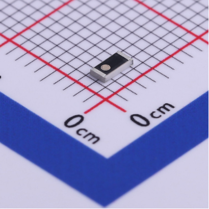
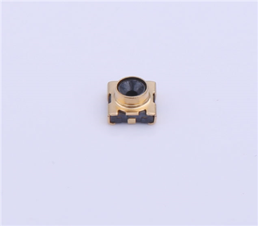
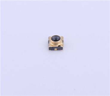
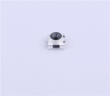
Thanks to its "compact size + high stability," the Bluetooth ceramic chip antenna has become an essential wireless component in miniature devices like smartwatches and Bluetooth earbuds. Despite being as small as a fingernail (as little as 3mm × 5mm), it enables stable communication over 10 meters. Behind this performance lies a sophisticated structural design. This article provides a comprehensive analysis of the Bluetooth ceramic chip antenna—from core structure, material properties, and key parameters to performance-affecting factors—revealing how it achieves powerful communication in miniature formats.
The performance of a Bluetooth ceramic chip antenna is determined by a laminated structure, where each layer serves a critical function. Even a dimensional deviation of 0.1mm can result in more than 30% signal loss.
Primary Function: Supports the entire antenna structure and adjusts the signal wavelength through dielectric constant (εr), enabling efficient radiation in compact form factors.
Material Properties:
Main material: Alumina ceramic (Al₂O₃) with 90%-96% purity (the higher the purity, the more stable the dielectric constant—within ±1).
Dielectric constant εr = 10–90 (commonly 20–30, which is 5–8 times that of FR4), compressing the 2.4GHz wavelength to 1/√εr of its original length (e.g., εr = 25 shortens the wavelength to 1/5, allowing antenna size to shrink to 1/4 of an FR4 antenna).
Low thermal expansion coefficient (<8ppm/°C), ensuring size stability from -40°C to 85°C (frequency drift ≤±5MHz).
Structural Details: Thickness 0.5–2mm (typically 1mm); surface must be polished (Ra ≤ 0.1μm) to ensure close bonding with metal layers.
Primary Function: Converts RF current from the Bluetooth module into 2.4GHz electromagnetic waves—acts as the “signal outlet.”
Material & Process:
Made of oxygen-free copper foil (99.9% purity), applied via thick-film printing or sputtering. Thickness: 3–10μm (too thin = oxidation risk, too thick = poor precision).
Typically rectangular or polygonal (shaped via etching), with size directly tied to frequency—at 2.4GHz, edge length ≈ 1/4 of the compressed wavelength (e.g., εr = 25 → compressed λ = 25mm → edge ≈ 6.25mm).
Key Design Notes:
Rounded corners (radius 0.2–0.5mm) reduce signal reflection and improve VSWR by 0.3–0.5.
High-end models may have a nickel coating (1–2μm) on the radiating element for oxidation resistance (extends lifespan from 1 year to over 3 years).
Primary Function: Reflects downward EM waves back into free space (prevents absorption by internal metals), while providing stable ground reference to enhance radiation efficiency.
Structural Features:
Located on the opposite side of the ceramic substrate (facing the radiating element), made from the same oxygen-free copper foil.
Area ≥1.5× that of the radiating element (e.g., 5mm × 5mm radiating → ≥8mm × 8mm ground).
Connected to the device’s PCB ground through ground vias (diameter: 0.3–0.5mm); target ground resistance <0.05Ω (high resistance causes signal reflection).
Performance Impact: Insufficient ground area reduces radiation efficiency from 70% to below 50%, and causes radiation pattern “nulls” (signal drops >10dB at specific angles).
Primary Function: Protects the radiating and grounding layers from oxidation, abrasion, moisture, and dust—critical in humid environments.
Common Materials:
Epoxy Coating (10–30μm): Low-cost, good insulation, ideal for indoor use (e.g., fitness bands).
Aluminum Nitride Film (5–10μm): High temperature (>200°C) and corrosion resistant, ideal for industrial/automotive settings.
No Protection Design: Some ultra-compact antennas (<4mm × 4mm) omit protection layers to save space, requiring sealed housing (e.g., potting).
Note: Excessive protection thickness (>50μm) increases dielectric loss, leading to 5–10% signal attenuation, so thickness must be tightly controlled.
Understanding how structure affects performance helps diagnose signal issues quickly.
Rule: Each 0.1mm increase in the radiating edge size lowers the center frequency by 8–10MHz (based on εr = 25).
Example: Target frequency = 2.45GHz. If actual size is 3.2mm instead of 3.1mm, frequency drops to ~2.37GHz—outside Bluetooth band (2.4–2.485GHz), causing 15dB signal loss.
Fix: Add a “tuning stub” (~0.5mm × 0.2mm) to the edge. Each 0.1mm increases lowers frequency by 3–5MHz.
Rule: Higher εr allows smaller size but narrows bandwidth.
Comparison:
|
Dielectric Constant (εr) |
Antenna Size |
Bandwidth |
|
20 |
Large |
Wide |
|
40 |
Medium |
Medium |
|
60 |
Small |
Narrow |
Risk: High-εr ceramics (εr > 50) are temperature-sensitive: every 10°C rise can shift frequency by 3–5MHz. Requires temperature compensation circuitry.
Rule: Increasing ceramic thickness by 0.1mm lowers impedance by 5–8Ω (based on εr = 20).
Use Case: If the Bluetooth module output is 50Ω and antenna measures 60Ω, increasing substrate thickness from 1.0mm to 1.2mm can bring it down to ~52Ω, reducing VSWR from 1.8 to 1.3.
Note: Thickness >2mm increases size, compromising miniaturization. Recommended range: 0.5–1.5mm.
Cause: Photolithography inaccuracies (line width deviation >0.05mm) or low etchant concentration.
Impact: Impedance shifts (e.g., design = 50Ω, actual = 70Ω), return loss S11 worsens from -15dB to -8dB (50% more signal reflection).
Check: Inspect radiator edge with a 50× magnifier—burrs or copper residue = defect.
Cause: Uneven sintering temperatures or mechanical stress during packaging (e.g., >350°C soldering causes ceramic embrittlement).
Impact: Cracks disturb EM field, distort radiation pattern (dead spots), and can cause total failure.
Check: Shine a strong light through the substrate. Visible hairlines = cracks. Or use a multimeter to test for short between radiator and ground (should be insulated).
Cause: Uneven via plating (<0.5μm) or incomplete solder fill.
Impact: Ground resistance increases from 0.05Ω to >1Ω. Radiation efficiency drops by 20–30%, signal becomes unstable (fluctuations ±5dB).
Check: Use impedance meter to measure resistance between ground pad and device ground. >0.1Ω = likely cold joint.
Cutting 0.5mm × 0.5mm right angles at two diagonal corners of a rectangular radiator forms an octagon, improving EM field continuity and widening bandwidth from 60MHz to 75MHz (ideal for Bluetooth 5.0).
Engraving a 0.2mm wide ring slot 0.5mm from the ground edge reduces metal-induced interference (e.g., near battery/shielding cans), improving signal stability by ~15% (fluctuation from ±4dB → ±3dB).
The structural design of a Bluetooth ceramic chip antenna is a fusion of material science and electromagnetic theory. High dielectric ceramics enable miniaturization, precise radiator dimensions ensure frequency matching, and well-designed ground layers enhance efficiency.
Understanding these structural details helps avoid “small-size, poor-performance” traps during selection, and allows designers to optimize antenna layout (e.g., distance from metal, installation angle) for over 90% performance utilization.
If your device suffers from weak Bluetooth signals (e.g., RSSI < -80dB at 10 meters), first check the antenna structure for defects (e.g., radiator burrs, poor grounding), or optimize structural parameters like substrate thickness and radiator size.
Copyright © Shenzhen Kinghelm Electronics Co., Ltd. all rights reservedYue ICP Bei No. 17113853