Service hotline
+86 0755-23615795

Release date:2025-07-22Author source:KinghelmViews:82
RF PCBs, or Radio Frequency Printed Circuit Boards, are specialized types of PCBs designed to receive and transmit radio signals within a certain frequency range. These boards form the backbone of a variety of modern electronics and communication systems, including mobile phones, radar systems, GPS devices, and wireless networks. Unlike their everyday counterparts, RF PCBs operate at high frequencies and require meticulous design, specific materials, and specialized manufacturing techniques.
This article delves into the world of RF PCBs, exploring design considerations for ensuring signal integrity, materials that meticulously reduce signal loss, and the complex processes that bring these high-performance circuit boards to life. By understanding these aspects, we gain deeper insight into the complexity and ingenuity behind connecting our devices in the wireless world.
The difference between RF PCBs and standard PCBs lies in their ability to handle high-frequency signals, typically ranging from 500 MHz to 2 GHz and beyond. This capability is crucial for minimizing signal loss and ensuring signal integrity across a wide frequency range. Designing and manufacturing RF PCBs require precise control of dielectric constant and dissipation factor to achieve optimal high-frequency performance.
In high-speed RF PCBs, specific types of vias, such as blind vias and through-hole techniques, are used to effectively reduce signal loss and maintain controlled impedance. Additionally, the ground plane plays a vital role in minimizing noise and ensuring a stable reference for RF traces.
The importance of frequency in RF PCB applications cannot be overstated. High-frequency signals are more prone to loss and require careful consideration of PCB layout, material selection, and component placement to effectively reduce signal attenuation and electromagnetic interference (EMI). For instance, the choice of substrate material is key to determining how efficiently the board transmits RF signals. Materials with low dielectric constant and dissipation factor are preferred to reduce signal loss and support higher-frequency applications.
RF PCBs are critical in modern technologies where wireless communication is essential. These include, but are not limited to, mobile communication devices, radar systems, GPS units, wireless network equipment, and satellite communication systems. The ability of RF PCBs to manage high-frequency signals effectively makes them indispensable in the development and operation of these technologies.
RF PCBs typically include antennas, filters, and amplifiers, each serving a unique RF function. Antennas are essential for transmitting and receiving electromagnetic signals. Their design and placement on the PCB significantly impact system range and efficiency. Filters play a critical role in selecting and isolating frequencies of interest, ensuring the device operates within its designated frequency band while rejecting unwanted signals. Amplifiers, on the other hand, increase the strength of weak signals to ensure they can be effectively processed without being overwhelmed by noise.

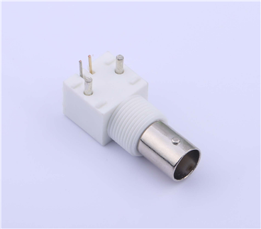
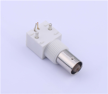
RF antenna connections on the PCB
Within an RF PCB, each component works together to achieve the desired functionality. For example, in wireless communication devices, an antenna receives incoming RF signals, which are then passed through filters to isolate the signals of interest. The filtered signals can then be amplified to an appropriate level for processing by the device's circuits. This interaction is carefully designed to optimize RF system performance, considering factors such as signal strength, bandwidth, and interference.
Electromagnetic Wave Propagation:
RF signals propagate as electromagnetic waves along PCB traces. These waves consist of electric and magnetic fields traveling together. The design of the trace geometry, the dielectric material between layers, and the surrounding environment all affect how these waves travel.
Signal Integrity:
Maintaining clean and undistorted signals is critical in RF applications. Signal integrity refers to the signal's ability to travel from its source to its destination on the PCB with minimal distortion or loss. Factors such as impedance mismatch, crosstalk, and signal attenuation can significantly degrade signal integrity.
Controlled Impedance:
Impedance is the opposition a signal encounters as it travels along a conductor. Maintaining controlled impedance in RF PCBs is crucial. Deviations from the desired impedance can cause signal reflection, leading to power loss and data distortion. Microstrip design requires careful consideration of trace width, substrate properties, and thickness to achieve the target impedance.
High-Frequency Materials:
Standard FR4 material, commonly used in everyday PCBs, encounters problems at high frequencies. RF PCBs often use specialized substrates with lower dielectric constants to reduce signal loss. Materials such as PTFE (Polytetrafluoroethylene), Rogers RT Duroid, or Taconic provide excellent electrical performance for high-frequency applications.
Signal Loss Mechanisms:
Several mechanisms cause signal loss on RF PCBs at high frequencies, including:
lConductor loss: Some signal power dissipates as heat due to the resistance of the copper traces themselves.
lDielectric loss: The dielectric material between layers absorbs part of the signal energy.
lRadiation loss: A small portion of signal energy may radiate away from the traces if not properly contained.
By understanding the science of signal propagation, impedance control, and material properties, RF PCB designers can create high-performance boards that enable seamless wireless communication.
Manufacturing RF PCBs involves using various materials, each selected for its specific properties suitable for high-frequency applications. Common materials include FR4, Rogers materials, PTFE, hydrocarbon resins, and ceramic substrates.
FR4 is a standard material in PCB manufacturing due to its cost-effectiveness and good performance at lower frequencies. However, its higher dielectric constant and dissipation factor make it less suitable for high-frequency RF applications, as it can cause significant signal loss and dispersion.

Rogers materials used for RF PCBs
Rogers materials are a family of high-frequency laminates offering lower dielectric constant and dissipation factor compared to FR4. These properties make Rogers materials a preferred choice for RF PCBs, as they significantly reduce signal loss and support higher frequency ranges. Rogers materials also exhibit low moisture absorption, which helps maintain stable electrical performance under varying environmental conditions.
PTFE, known for its very low dielectric constant and dissipation factor, is another widely used RF PCB material, particularly in high-frequency applications. Teflon’s outstanding electrical performance ensures minimal signal loss and phase shift, making it ideal for critical RF applications. However, its softness and higher cost can pose challenges in PCB manufacturing and limit its use to specific high-performance applications.
Ceramic substrates offer high thermal conductivity, excellent dielectric properties, and superior mechanical stability, making them suitable for high-power RF applications. Their ability to withstand high temperatures and maintain stable electrical performance under thermal stress is especially beneficial where heat dissipation must be considered.

Ceramic substrates in PCBs
The choice of material significantly impacts RF PCB performance. While FR4 may be sufficient for lower frequencies or less critical applications, the superior electrical properties of Rogers materials, PTFE, and ceramic substrates make them better suited for high-frequency, high-performance designs. PTFE's higher coefficient of thermal expansion (CTE) requires careful design consideration when used in RF PCBs. The decision between these materials involves balancing cost, performance, and manufacturability to meet specific application requirements.
RF PCB design requires careful consideration of signal integrity, controlled impedance, and minimal signal loss. Unlike standard PCBs, RF designs place particular emphasis on trace geometry, material selection, and component layout.

RF energy harvesting system
Impedance matching is critical for minimizing signal reflection and ensuring maximum power transfer between components. This is often achieved by carefully designing trace widths and using simulation tools to calculate the precise impedance. Even slight deviations from the target impedance can lead to significant signal degradation at high frequencies.
Grounding and shielding are also key design elements. A solid ground plane reduces noise, provides a stable reference for RF signals, and minimizes electromagnetic interference (EMI). In multilayer boards, careful separation of RF and digital signals helps reduce crosstalk and preserves signal integrity.
Trace geometry directly affects impedance and signal propagation. Designers often use microstrip or stripline configurations to achieve controlled impedance. Trace spacing, width, and the dielectric properties of the substrate must be balanced to maintain the desired impedance throughout the circuit.

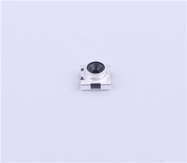
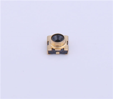
RF PCB module
Component placement and routing must consider high-frequency behavior. Components like filters, amplifiers, and antennas should be positioned to minimize signal path lengths and reduce parasitic inductance and capacitance. Additionally, the use of vias must be carefully managed. Excessive or poorly placed vias can introduce unwanted signal reflections and losses.
EMI considerations are vital for RF PCB design. Proper shielding, via fences, and careful routing help prevent unwanted emissions and reduce susceptibility to external noise sources. Designers often use metal enclosures or shielding cans to isolate sensitive RF circuits.
By addressing these design considerations, engineers can create RF PCBs capable of maintaining performance across a wide range of operating conditions and frequencies.
Simulation and modeling are indispensable tools in RF PCB design, helping predict real-world performance before physical prototyping. Engineers use electromagnetic (EM) simulation software to model trace impedance, evaluate electromagnetic fields, and analyze potential sources of interference.
3D EM simulation provides detailed insights into complex RF structures like antennas, couplers, and filters. These simulations help visualize field distribution and identify design flaws that may not be apparent from schematic analysis alone.
Time-domain and frequency-domain analysis are used to understand how RF signals behave over the board's entire frequency range. This allows designers to optimize layout, trace lengths, and component placement for best performance.
Simulation also aids in validating impedance matching networks and filter designs, ensuring they meet target specifications before manufacturing. By reducing the number of prototype iterations needed, simulation significantly cuts development time and cost.
RF PCBs demand specialized manufacturing techniques to maintain the high precision and performance required at radio frequencies.
Layer stacking and lamination:
The stack-up design must account for controlled impedance and minimal dielectric loss. Laminating high-frequency materials like PTFE or Rogers laminates requires specialized processes to handle their unique thermal properties.
Precision etching:
At high frequencies, even small variations in trace width or spacing can impact impedance and signal performance. Advanced photolithography and etching techniques are used to achieve the precise geometries necessary.
Via formation:
Techniques like laser drilling enable the creation of blind and buried vias, which help reduce parasitic effects and support high-density designs.
Surface finishes:
Finishes like ENIG (Electroless Nickel Immersion Gold) or silver are often used on RF boards to ensure stable conductivity and prevent oxidation, which can degrade signal quality.
Inspection and testing:
RF PCBs undergo strict quality control, including automated optical inspection (AOI), electrical testing, and often RF performance testing, to ensure compliance with design specifications.
Quality control is critical for RF PCBs due to their sensitivity to even minor defects.

Automated Optical Inspection (AOI) for PCB Assembly
Electrical testing verifies continuity and ensures there are no open or short circuits. Controlled impedance testing confirms that the manufactured impedance matches the design targets.
RF performance testing often includes measurements of insertion loss, return loss, and phase stability across the intended frequency range. These tests identify potential problems like excessive signal loss, impedance mismatches, or parasitic effects.
Environmental testing, including thermal cycling and humidity exposure, helps ensure the PCB maintains performance under real-world conditions. This is especially important for RF applications that may experience temperature fluctuations or outdoor use.
By combining design verification, process control, and rigorous testing, manufacturers deliver RF PCBs that meet both performance and reliability requirements.
The RF PCB industry continues to evolve alongside advances in wireless technology.
5G technology requires PCBs capable of supporting millimeter-wave frequencies, often above 24 GHz. This demands even tighter manufacturing tolerances, lower-loss materials, and innovative design approaches.
Flexible and rigid-flex RF PCBs are increasingly popular in compact devices like smartphones and wearables, where they enable more complex designs and space savings.

Flexible RF PCB
High-density interconnect (HDI) technology supports the integration of more RF functionality into smaller footprints, improving device performance and enabling more sophisticated wireless systems.
Material innovation continues to focus on substrates with even lower dielectric loss and better thermal stability, further enhancing high-frequency performance.
As the demand for faster, more reliable wireless communication grows, RF PCB design and manufacturing will keep advancing, driving the next generation of connected technologies.
RF PCBs are far more than just circuit boards—they are critical enablers of the wireless world. From the choice of specialized materials to careful design, simulation, and advanced manufacturing, every step contributes to their ability to handle high-frequency signals with minimal loss and distortion.
By understanding the science, design challenges, and technologies behind RF PCBs, we can better appreciate the complex engineering that keeps us connected—from smartphones and satellites to radar systems and beyond. As wireless communication continues to evolve, RF PCBs will remain at the heart of innovation.
Disclaimer: This article is excerpted from Electronic Design Practitioner. The views expressed are solely those of the author and do not represent the opinions of Kinghelm or the industry. It is shared for the purpose of reposting and sharing only. We support the protection of intellectual property rights. Please indicate the original source and author when reposting. If there is any infringement, please contact us for removal.