Service hotline
+86 0755-23615795

Release date:2025-06-05Author source:KinghelmViews:1775
USB is a fast, bidirectional, synchronous, low-cost, hot-pluggable serial interface. Its advantages—high-speed data transfer, user-friendly design, and hot-swap support—have made USB devices ubiquitous. While USB 2.0 remains widely adopted, many hardware beginners encounter persistent issues, such as unstable communication or complete failure, even after verifying schematics and soldering. In such cases, suboptimal PCB design is often the culprit. Designing a PCB that meets USB 2.0 data transfer requirements is critical for performance and reliability.
The USB protocol transmits digital signals through a differential pair (D+, D-). For stable operation, these traces must strictly adhere to differential signaling rules. Based on years of design and debugging experience, key layout guidelines are summarized below:
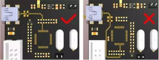
1. Minimize Trace Length:
l Place components to shorten differential paths (✓ Optimal, ✗ Suboptimal).
2. Prioritize Differential Routing:
l Use ≤ 2 vias per pair (vias increase parasitic inductance, degrading signal integrity).
l Place vias symmetrically (✓ Optimal, ✗ Suboptimal).

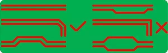
3. Symmetric & Parallel Routing:
l Ensure tight coupling; avoid 90° bends. Use arcs or 45° angles (✓ Optimal, ✗ Suboptimal).
4. Placement of Series R/C, Test Points & Pull-Up/Down Resistors:
l Position components to minimize stub effects (✓ Optimal, ✗ Suboptimal).

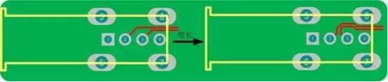
5. Length Matching:
l Mismatched lengths cause timing skew and common-mode noise. Compensate length differences ≤ 5 mil at the source of mismatch.
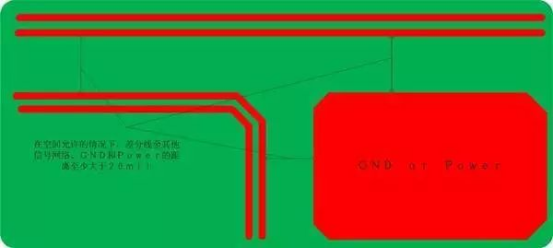
6. Crosstalk Mitigation:
l Maintain ≥ 20 mil clearance between diff pairs and other signals/ground pours (ground proximity affects impedance).
7. Power Trace Sizing:
l VBUS/GND must handle 500 mA. For 1-oz copper, ≥ 20 mil width suffices (wider traces improve power integrity).
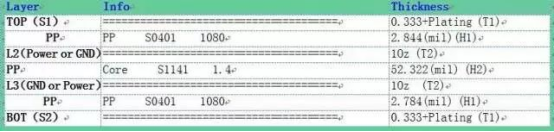
While the above rules suffice for low-speed USB, high-speed operation (480 Mbps) requires impedance-controlled differential pairs. Key considerations:
l Target Impedance: 90 Ω ± 10% (refer to IC datasheet).
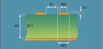
l Impedance Depends On:
n Inversely: Trace width (W1, W2), copper thickness (T1), dielectric constant (Er1).
n Directly: Trace spacing (S1), distance to reference layer (H1).
|
Layer |
Function |
Note |
|
Top |
Signal |
USB diff pairs routed here |
|
Mid1 |
Ground (GND) |
Must be unbroken under diff pairs |
|
Mid2 |
Power (VCC) |
Reference plane |
|
Bottom |
Signal |
l For 90 Ω impedance in this stackup:
n Trace Width: 4.5 mil
n Trace Spacing: 5.5 mil
l Note: Board manufacturers may adjust these values based on material properties and process capabilities.
For robust USB 2.0 performance:
1. Route differential pairs short, tightly coupled, length-matched, and impedance-controlled.
2. Ensure adequate VBUS/GND trace width for current handling.
3. Maintain a continuous reference plane beneath diff pairs.
Adhering to these principles resolves most USB interface stability issues.
Note: This article is sourced from the internet and does not reflect the views of Kinghelm or the industry as a whole. It is shared for informational purposes only. We support the protection of intellectual property rights—please credit the original source and author when sharing. If you believe this content infringes on your rights, kindly contact us for removal.
Copyright © Shenzhen Kinghelm Electronics Co., Ltd. all rights reservedYue ICP Bei No. 17113853