Service hotline
+86 0755-23615795

Release date:2025-08-04Author source:KinghelmViews:239
In compact devices like Bluetooth earbuds and smartwatches, a thumbnail-sized Bluetooth chip antenna serves as the “core organ” enabling wireless communication. But how does it convert an electrical signal into an electromagnetic wave that can travel hundreds of meters? And why can antennas of the same size differ in signal strength by up to threefold?
This article explains the principle of Bluetooth chip antennas, from structural design and working mechanism to critical performance parameters—helping you understand their essential role in device communication.

The performance of a Bluetooth chip antenna fundamentally depends on its physical structure, which consists of three indispensable parts:
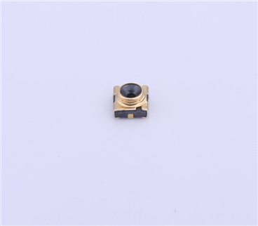
The radiator is the antenna’s “signal outlet,” typically made from etched copper foil (thickness 0.01–0.03 mm). It often has a rectangular, circular, or irregular polygon shape. Its area directly relates to the Bluetooth frequency band: at 2.4 GHz (wavelength ≈ 12.5 cm), the radiator length is typically about 1/4 wavelength (~3.1 cm) or 1/2 wavelength (~6.2 cm). By adjusting dimensions, it precisely matches the 2.4–2.485 GHz operating frequency.
For example, a 5 mm × 5 mm ceramic chip antenna uses a folded rectangle pattern in the radiator to achieve an effective 1/4 wavelength within its compact size, ensuring efficient radiation at the 2.44 GHz Bluetooth center frequency.
The substrate is the radiator’s supporting platform and directly affects gain and frequency stability. Common substrates include:
lCeramics: High dielectric constant (εr=20–90), allowing smaller antenna size (≈30% smaller than FR4), but fragile—suited for precision devices like medical sensors.
lFR4 fiberglass: Low cost, easy processing, stable dielectric constant (εr=4.2–4.8), common in consumer electronics like Bluetooth speakers.
lFPC (Flexible Printed Circuit): Materials like LCP (Liquid Crystal Polymer), bendable (radius ≥1 mm), lower dielectric constant (εr=2.9–3.2), ideal for curved surfaces like fitness bands.
Higher dielectric constants reduce radiator size but can lower radiation efficiency (e.g., ceramic antennas ~60%, FR4 antennas ~75%).
The ground plane is a large metal layer below the antenna, connected to the device ground. Its role is like a mirror:
lReflects downward electromagnetic waves from the radiator upward, improving total radiation efficiency by 30–50%.
lThe ground plane should be at least three times the radiator area (e.g., for a 10 mm × 10 mm radiator, ≥30 mm × 30 mm). Otherwise, reflection weakens, and signal directionality issues can occur (up to 20 dB drop in some directions).
A Bluetooth chip antenna is essentially an energy converter, with three critical steps—all happening in nanoseconds:
The Bluetooth chip outputs an RF signal (2.4–2.485 GHz) through a feed line (e.g., 50Ω microstrip) to the feed point (the metal contact where radiator meets substrate). This is an alternating current (AC) where electrons oscillate at 2.4 billion times per second.
As AC flows through the radiator, it generates a high-frequency alternating electromagnetic field around it:
lNear Field (within ~2 cm or 1/6 wavelength): Energy alternates between electric and magnetic fields, not yet radiating.
l Far Field (>2 cm): The electromagnetic field detaches and propagates outward as an electromagnetic wave at the speed of light (≈3×10⁸ m/s).
Think of this like ripples on water: the radiator vibrates electrically, creating expanding waves.
The antenna’s radiation pattern is shaped by the radiator’s position relative to the ground plane:
lTypical flat chip antennas (radiator parallel to ground): Produce a doughnut-shaped omnidirectional pattern—360° horizontal coverage, with two vertical lobes; suitable for all-around communication like gateways.
lBent chip antennas (FPC materials, radiator at ~30° angle): Focus energy toward the bend, increasing gain by 2–3 dBi; suited for directional uses like earbuds facing a phone.
Understanding these parameters helps connect design to real-world performance:
Gain measures how much the antenna “focuses” energy in a direction (unit: dBi):
lOmnidirectional Bluetooth chip antennas: usually 0–2 dBi, good for even coverage at short range.
lDirectional designs: 3–5 dBi, extending range (e.g., from 10 m to 15 m) but narrowing beam width to ~120°.
Higher gain means the radiator more efficiently “concentrates” energy—like a flashlight focusing its beam.
VSWR shows how well the antenna impedance matches the Bluetooth module’s 50Ω:
lIdeal VSWR=1; practical requirement ≤1.5.
lIf perfectly matched, nearly all signal radiates outward.
lIf mismatched (e.g., due to dielectric constant deviation raising impedance to 70Ω), part of the signal reflects back, reducing efficiency (e.g., from 70% down to 40%).
Bandwidth is the range over which the antenna performs efficiently, needing to cover Bluetooth’s 2.4–2.485 GHz (≥85 MHz):
lCeramic antennas: often narrower (~50–70 MHz), so small frequency shifts (±20 MHz from temperature) can drop gain by over 3 dB.
lFR4 or FPC antennas: wider bandwidth (≥100 MHz), better for industrial or temperature-variable environments.
For space-constrained designs (e.g., earbuds), high εr ceramic substrates (e.g., εr=90) shrink antennas to 3 mm × 3 mm—but with ~0.5–1 dBi lower gain, which can be partly offset by optimizing radiator shape.
Because metal absorbs electromagnetic waves:
lKeep at least 3 mm of space around the antenna free from batteries, shields, or other metal parts.
lIf unavoidable (e.g., metal watch housing), add a ~0.5 mm air gap (εr=1) between antenna and metal to reduce absorption.
Dielectric constant shifts with temperature (e.g., ceramic εr may deviate ±2 over -40–85°C), shifting the frequency:
lUse low-temperature-coefficient substrates (e.g., LCP, <±10 ppm/°C).
lAdd tuning stubs (small metal tabs) at radiator edges for capacitive compensation.
At its core, a Bluetooth chip antenna works by transforming high-frequency electrical currents in the radiator into propagating electromagnetic waves. The structure—radiator, substrate, ground—directly affects signal strength, coverage, and stability.
Understanding these principles helps you:
lChoose the right substrate (e.g., FPC for curved designs, ceramic for precision).
lOptimize layout (avoid metal, ensure ground size).
lQuickly troubleshoot issues (e.g., high VSWR may signal impedance mismatch).
If you’d like to optimize Bluetooth signal performance (e.g., longer range or better anti-interference), share your device size and use case—and get design suggestions grounded in these principles.
Copyright © Shenzhen Kinghelm Electronics Co., Ltd. all rights reservedYue ICP Bei No. 17113853