

Service Hotline
Resources

Resources
What Is a Female Header? Types, Uses, and PCB Selection Guide
2026-06-11
30
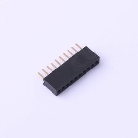 A female header connector is a PCB or cable connector whose contacts are hollow sockets — designed to receive the pins of a mating male header. It is one of the most common interconnect components in electronics, found everywhere from Arduino shields to industrial control boards.
This guide is for: PCB designers, embedded systems engineers, and makers who need to understand, select, or solder female headers correctly.
Not covered: High-current power connectors, RF/coaxial connectors, or crimp-tool assembly of wire harnesses — these fall outside the standard pin-header family and have separate selection criteria.
What Is a Female Header?
A female header consists of a row (or grid) of spring-loaded socket contacts housed in a plastic insulator body. Each socket is sized to receive a standard male pin. The term "female" describes the receptive contact geometry — the pin inserts into the socket — consistent with IEC 60050-151 general connector terminology.
Three parameters you must confirm before ordering any female header PCB component:
- Pitch:center-to-center distance between adjacent contacts. The global standard for general-purpose headers is 54 mm (0.1 inch); 2.00 mm and 1.27 mm are common in compact designs.
- Pin count and row count:single-row (1×N) or double-row (2×N).
- Contact plating:tin plating suits most signal/low-frequency applications; gold plating improves reliability in low-current or high-cycle-count connections.
Female Header Types
Choosing the wrong type is a common and avoidable design error. The table below covers the main female header types found in production and prototyping:
|
Type |
Configuration |
Typical Application |
|
Single-row (SIL) |
1×N sockets |
GPIO breakouts, edge connectors |
|
Double-row (DIL) |
2×N sockets |
IC sockets, dense board-to-board links |
|
Right-angle |
Contacts exit at 90° to PCB |
Panel-edge access, low-profile enclosures |
|
SMD (surface-mount) |
Solders to surface pads |
High-density layouts, automated assembly |
|
Stackable / low-profile |
Extended insulator body |
Arduino-style shield stacking |
|
Wire-to-board housing |
Off-board, crimped terminals |
Cable harnesses, peripheral wiring |
Pitch and type are independent variables — always confirm both against your mating male header's datasheet before placing an order.
What Is a Female Header Connector Used For?
Female header connectors serve three primary functions:
- Board-to-board stacking.A female header on a base board accepts a male header on a daughter board, enabling modular, reversible expansion. The Arduino shield ecosystem is the most widely recognized example of this pattern.
- Module-to-board interfacing.Sensor modules, display modules, and wireless modules typically ship with male pin headers. Soldering a female header onto a carrier PCB lets you swap or replace modules without desoldering — a significant advantage during prototyping and field maintenance.
- Cable-to-board connections.Female housing connectors (Dupont-style or JST-compatible) terminate flying leads for connecting peripherals. This approach is common in low-to-mid volume production where connectorized cables simplify assembly and service.
Female Header vs. Male Header
|
Attribute |
Female Header |
Male Header |
|
Contact geometry |
Socket (receives pin) |
Pin (inserts into socket) |
|
Exposed metal when unmated |
No — contacts recessed |
Yes — pins exposed |
|
Short-circuit risk when unmated |
Lower |
Higher |
|
Rework ease |
Moderate |
Easier (pins visible) |
|
Typical PCB role |
Receiving / mating side |
Source / plug side |
Placement convention: There is no universal rule mandating which gender goes on which board. A common engineering practice is to place the female (recessed) connector on the side that carries a live power rail when unmated, since the recessed geometry reduces accidental short-circuit risk. Your specific mechanical layout and safety requirements should drive the final decision — not convention alone.
How to verify your placement choice: Before finalizing layout, check whether the unmated connector will be accessible to a user or exposed in the enclosure. If so, the recessed female contact reduces — though does not eliminate — shock and short-circuit hazard. Confirm against your product's applicable safety standard (e.g., IEC 60950-1 / IEC 62368-1 for IT and AV equipment).
How to Solder Female Header Pins
This procedure applies to through-hole female headers on standard FR4 PCBs. SMD variants require controlled reflow and are outside this scope.
Prerequisites:
- Temperature-controlled soldering iron (320–370 °C for leaded solder; 340–380 °C for lead-free SAC305)
- Solder wire, 0.8–1.0 mm diameter
- No-clean or rosin-core flux
- PCB with correct footprint (hole diameter ~0.9–1.0 mm for 2.54 mm pitch standard headers)
- PCB holder or helping hands
Steps:
- Dry-fit first.Insert the header into the footprint without solder. It should seat flush with no forcing. A tight fit suggests an incorrect hole size — stop and verify the footprint before proceeding.
- Tack one corner pin.Apply a small solder amount to a single end pin while holding the header flush. This anchors position for the remaining pins.
- Check perpendicularity.Inspect from both the side and front. Reheat the tack joint and adjust if the header is tilted — this is your last easy correction point.
- Solder remaining pins sequentially.Place the iron tip at the pin/pad junction for approximately 2 seconds, then feed solder wire into the joint (not onto the iron tip). A good joint is shiny, smooth, and forms a concave fillet that wets both pin and pad annular ring.
- Inspect every joint.Use a magnifier or phone camera. Reject joints that are: dull or grainy (cold joint), balled up without pad wetting (insufficient heat), or bridging to an adjacent pin.
- Clean flux residueper your product's requirements. No-clean flux is acceptable in many assemblies per IPC-A-610 guidelines, but confirm with your quality specification.
Failure signals and what they indicate:
- Intermittent connection after mating:likely a cold joint — reflow with added flux
- Header tilted after full soldering:tack joint cooled before alignment check — desolder, clean, and restart from step 2
- Solder bridges between pins:remove with solder wick and flux, re-inspect under magnification
How to verify: After soldering, use a multimeter in continuity mode to confirm each pin connects to its intended net. For applications with repeated mating cycles (>50), a brief functional insertion/removal test under operating conditions can reveal marginal mechanical joints before the board ships.
Related Recommendations