

Service Hotline
Resources

Resources
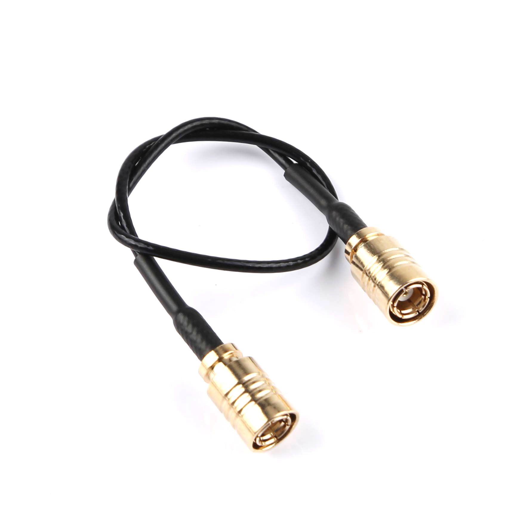
SMB Cable Assembly Guide: Choosing, Assembling, and Optimizing SMB RF Coaxial Cables for Reliable Performance
2026-06-17
36
What Is an SMB Cable Assembly?
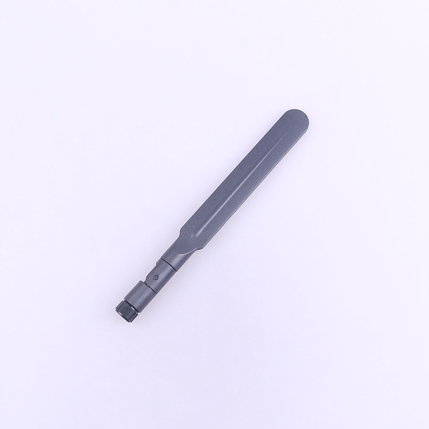
SMB cable assemblies consist of SMB connectors terminated on coaxial cables designed for radio frequency (RF) signal transmission. SMB stands for SubMiniature version B, a snap-on coaxial connector series known for its compact size, quick mating, and reliable performance up to approximately 4 GHz (with some extended designs reaching higher).
These assemblies are widely used in automotive electronics, GPS systems, telecommunications, test equipment, and other space-constrained RF applications. Unlike threaded connectors such as SMA, SMB uses a snap-on mechanism for faster connect/disconnect cycles, making it ideal for applications requiring frequent mating or blind mating.
Who This Guide Helps: Engineers selecting or assembling components for prototypes or production, and decision-makers evaluating suppliers for volume RF interconnect solutions. It is less suitable for ultra-high-frequency microwave designs (>10 GHz) or high-vibration environments without additional strain relief.
SMB Connector Basics and Key Specifications
SMB connectors typically feature 50 Ω impedance (75 Ω variants exist for specific video/broadcast uses). Standard performance includes:
Frequency range: DC to 4 GHz
Voltage rating: Around 335 V RMS
Mating cycles: Minimum 500
Coupling: Snap-on (push-to-mate, pull-to-disconnect)
Note that in SMB convention, the plug (male) often has the female receptacle contact, while the jack has the male pin—an important detail for compatibility.
Common cable types paired with SMB connectors include flexible options suited for tight routing:
RG316 SMB cable: Popular for its balance of flexibility, low loss, and durability in moderate-temperature environments.
37 SMB cableand RG1.78 SMB cable: Ultra-fine micro-coax variants for high-density, space-limited designs like internal GPS antenna routing.
These cables maintain 50 Ω characteristic impedance when properly terminated.
Common SMB Cable Configurations and Applications
SMB Male to SMB Male Cable: Straightforward interconnects for extending RF paths between modules. SMB Female to SMB Male Cable: Often used as extension or adapter cables. SMB Female to SMB Female Cable: Useful for linking male-ended equipment.
GPS Antenna SMB Cable assemblies are particularly common in automotive and navigation systems, where compact, reliable signal transfer from antenna to receiver is critical. RG174/RG316 or 1.37mm variants provide the necessary flexibility for vehicle installations.
In automotive electronics, SMB assemblies support infotainment, telematics, and sensor connections where vibration resistance and compact form factor matter.
How to Select the Right SMB Cable Assembly
Consider these decision factors:
Frequency and Loss Budget: Verify the assembly's insertion loss across your operating band. Shorter lengths and larger cable diameters (e.g., RG316 vs. RG1.37) reduce attenuation.
Environmental Conditions: Temperature range (-55°C to +165°C typical), vibration, and exposure. Use double-shielded or more robust jackets where needed.
Mechanical Constraints: Bend radius, cable flexibility, and connector orientation (straight vs. right-angle).
Power Handling and Impedance Matching: Ensure 50 Ω consistency end-to-end to minimize reflections (VSWR).
Volume and Customization: For production, evaluate supplier capabilities for custom lengths, labeling, and testing.
Verification Tip: Request VSWR, insertion loss, and return loss data from the manufacturer for your specific frequency and length. You can verify basic continuity and impedance with a vector network analyzer (VNA) or time-domain reflectometer (TDR) if available.
Step-by-Step SMB Cable Assembly Best Practices
Pre-Assembly Checks:
Select compatible cable and connector (e.g., crimp or solder type matched to RG316 or RG1.37).
Gather tools: Precision cable stripper, crimp tool with correct dies, heat gun for shrink tubing, and calipers for measurements.
Work in a clean environment to avoid contamination.
Typical Crimp Assembly Process (for common clamp/crimp SMB connectors):
Slide heat-shrink tubing and ferrule onto the cable.
Strip the cable to manufacturer-specified dimensions (center conductor, dielectric, braid—avoid nicking).
Flare or trim the braid evenly.
Insert into connector, ensuring proper seating of center conductor and braid contact.
Crimp the ferrule using the correct tool and die set.
Apply heat shrink for strain relief and insulation.
Always follow the specific connector manufacturer's assembly instructions, as dimensions vary slightly by cable type (RG316, RG178 equivalents, etc.).
Expected Results: Secure mechanical connection with no exposed braid or dielectric gaps, and stable electrical performance.
Verification: Perform a visual inspection, tug test for retention, and electrical tests (continuity, insulation resistance, VSWR if equipped).
Common Failure Signals and Diagnosis:
High VSWR or signal loss: Check for improper stripping, poor crimp, or damage.
Intermittent connection: Misalignment or insufficient braid contact—re-terminate.
Mechanical pull-out: Insufficient crimp force or wrong ferrule.
Comparison of Popular SMB Cable Types
Cable Type
Key Strengths
Best For
Considerations
RG316
Good flexibility, moderate loss
General RF, GPS extensions
Larger diameter than micro-coax
RG1.37
Ultra-compact, high density
Internal board-to-antenna routing
Higher loss over long runs
RG1.78
Balance of size and performance
Automotive, tight spaces
Similar to RG316 variants
Choose based on your loss budget and routing needs. Shorter runs favor smaller cables.
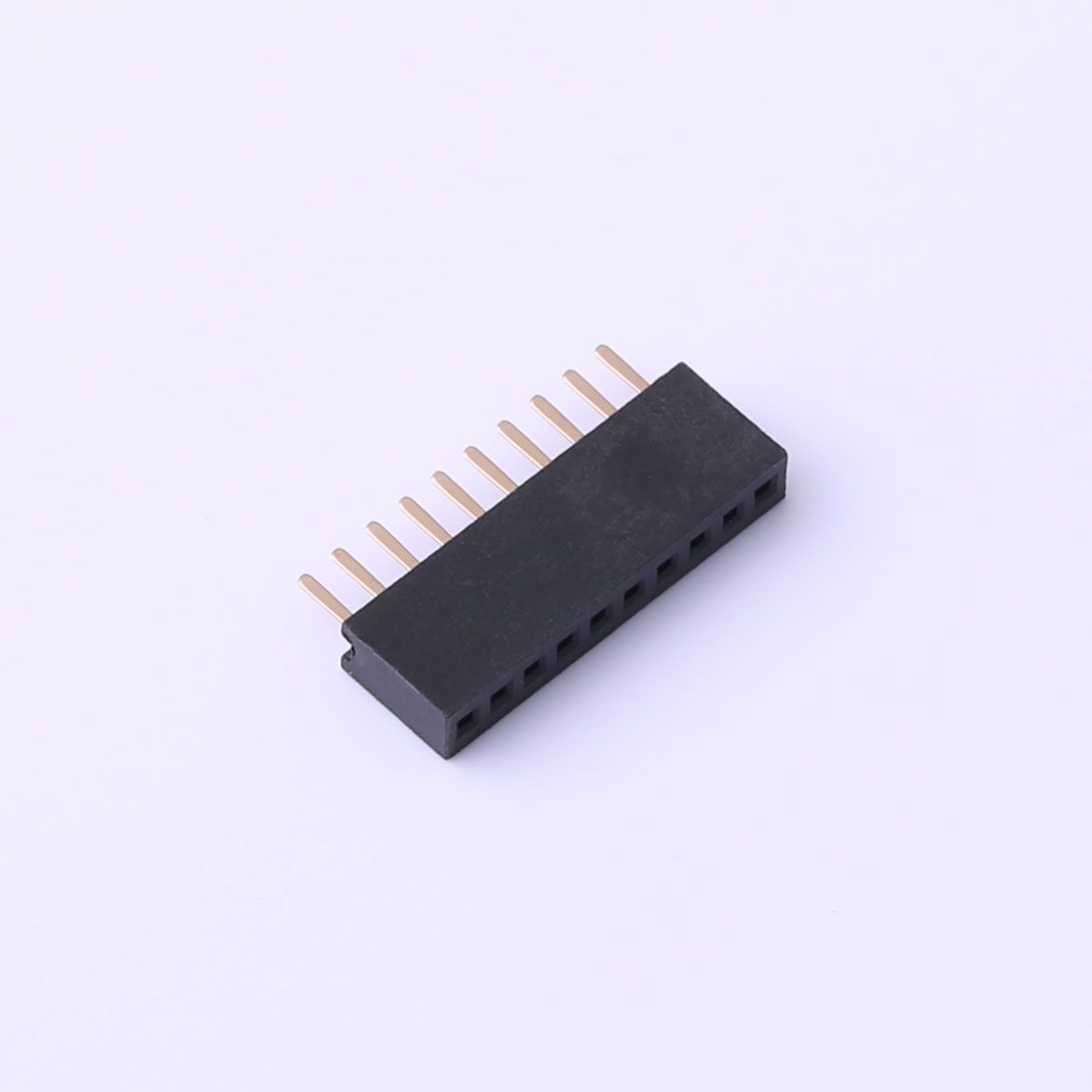
What Is a Female Header? Types, Uses, and PCB Selection Guide
2026-06-11
29
A female header connector is a PCB or cable connector whose contacts are hollow sockets — designed to receive the pins of a mating male header. It is one of the most common interconnect components in electronics, found everywhere from Arduino shields to industrial control boards.
This guide is for: PCB designers, embedded systems engineers, and makers who need to understand, select, or solder female headers correctly.
Not covered: High-current power connectors, RF/coaxial connectors, or crimp-tool assembly of wire harnesses — these fall outside the standard pin-header family and have separate selection criteria.
What Is a Female Header?
A female header consists of a row (or grid) of spring-loaded socket contacts housed in a plastic insulator body. Each socket is sized to receive a standard male pin. The term "female" describes the receptive contact geometry — the pin inserts into the socket — consistent with IEC 60050-151 general connector terminology.
Three parameters you must confirm before ordering any female header PCB component:
Pitch:center-to-center distance between adjacent contacts. The global standard for general-purpose headers is 54 mm (0.1 inch); 2.00 mm and 1.27 mm are common in compact designs.
Pin count and row count:single-row (1×N) or double-row (2×N).
Contact plating:tin plating suits most signal/low-frequency applications; gold plating improves reliability in low-current or high-cycle-count connections.
Female Header Types
Choosing the wrong type is a common and avoidable design error. The table below covers the main female header types found in production and prototyping:
Type
Configuration
Typical Application
Single-row (SIL)
1×N sockets
GPIO breakouts, edge connectors
Double-row (DIL)
2×N sockets
IC sockets, dense board-to-board links
Right-angle
Contacts exit at 90° to PCB
Panel-edge access, low-profile enclosures
SMD (surface-mount)
Solders to surface pads
High-density layouts, automated assembly
Stackable / low-profile
Extended insulator body
Arduino-style shield stacking
Wire-to-board housing
Off-board, crimped terminals
Cable harnesses, peripheral wiring
Pitch and type are independent variables — always confirm both against your mating male header's datasheet before placing an order.
What Is a Female Header Connector Used For?
Female header connectors serve three primary functions:
Board-to-board stacking.A female header on a base board accepts a male header on a daughter board, enabling modular, reversible expansion. The Arduino shield ecosystem is the most widely recognized example of this pattern.
Module-to-board interfacing.Sensor modules, display modules, and wireless modules typically ship with male pin headers. Soldering a female header onto a carrier PCB lets you swap or replace modules without desoldering — a significant advantage during prototyping and field maintenance.
Cable-to-board connections.Female housing connectors (Dupont-style or JST-compatible) terminate flying leads for connecting peripherals. This approach is common in low-to-mid volume production where connectorized cables simplify assembly and service.
Female Header vs. Male Header
Attribute
Female Header
Male Header
Contact geometry
Socket (receives pin)
Pin (inserts into socket)
Exposed metal when unmated
No — contacts recessed
Yes — pins exposed
Short-circuit risk when unmated
Lower
Higher
Rework ease
Moderate
Easier (pins visible)
Typical PCB role
Receiving / mating side
Source / plug side
Placement convention: There is no universal rule mandating which gender goes on which board. A common engineering practice is to place the female (recessed) connector on the side that carries a live power rail when unmated, since the recessed geometry reduces accidental short-circuit risk. Your specific mechanical layout and safety requirements should drive the final decision — not convention alone.
How to verify your placement choice: Before finalizing layout, check whether the unmated connector will be accessible to a user or exposed in the enclosure. If so, the recessed female contact reduces — though does not eliminate — shock and short-circuit hazard. Confirm against your product's applicable safety standard (e.g., IEC 60950-1 / IEC 62368-1 for IT and AV equipment).
How to Solder Female Header Pins
This procedure applies to through-hole female headers on standard FR4 PCBs. SMD variants require controlled reflow and are outside this scope.
Prerequisites:
Temperature-controlled soldering iron (320–370 °C for leaded solder; 340–380 °C for lead-free SAC305)
Solder wire, 0.8–1.0 mm diameter
No-clean or rosin-core flux
PCB with correct footprint (hole diameter ~0.9–1.0 mm for 2.54 mm pitch standard headers)
PCB holder or helping hands
Steps:
Dry-fit first.Insert the header into the footprint without solder. It should seat flush with no forcing. A tight fit suggests an incorrect hole size — stop and verify the footprint before proceeding.
Tack one corner pin.Apply a small solder amount to a single end pin while holding the header flush. This anchors position for the remaining pins.
Check perpendicularity.Inspect from both the side and front. Reheat the tack joint and adjust if the header is tilted — this is your last easy correction point.
Solder remaining pins sequentially.Place the iron tip at the pin/pad junction for approximately 2 seconds, then feed solder wire into the joint (not onto the iron tip). A good joint is shiny, smooth, and forms a concave fillet that wets both pin and pad annular ring.
Inspect every joint.Use a magnifier or phone camera. Reject joints that are: dull or grainy (cold joint), balled up without pad wetting (insufficient heat), or bridging to an adjacent pin.
Clean flux residueper your product's requirements. No-clean flux is acceptable in many assemblies per IPC-A-610 guidelines, but confirm with your quality specification.
Failure signals and what they indicate:
Intermittent connection after mating:likely a cold joint — reflow with added flux
Header tilted after full soldering:tack joint cooled before alignment check — desolder, clean, and restart from step 2
Solder bridges between pins:remove with solder wick and flux, re-inspect under magnification
How to verify: After soldering, use a multimeter in continuity mode to confirm each pin connects to its intended net. For applications with repeated mating cycles (>50), a brief functional insertion/removal test under operating conditions can reveal marginal mechanical joints before the board ships.

How to Choose a Bluetooth Antenna? From Patch to Ceramic — A Complete Selection Guide
2026-06-01
87
When working with Bluetooth modules, many users face common frustrations: weak signal strength, short transmission range, and poor penetration through walls. This often leads to the question: Can switching to a better antenna significantly improve Bluetooth performance?
The answer is yes — but only if you choose the right type. Picking the wrong antenna can result in worse signal quality, higher power consumption, or even damage to your module. This guide covers the main Bluetooth antenna types, performance comparisons, selection criteria, installation tips, and common pitfalls to help you make the right choice.
1. Main Types of Bluetooth Antennas and Their Characteristics
Bluetooth operates at 2.4GHz. Different antenna structures offer unique advantages and trade-offs. Here are the most common types currently available:
Patch AntennaCompact, low-cost, and easy to integrate. Often used as onboard or external small antennas.
Ceramic AntennaTiny chip-style ceramic antennas usually soldered directly onto the PCB. Smallest size but relatively low gain.
Rubber Duck AntennaThe classic flexible external antenna. Typical gain ranges from 2-5dBi with good cost-performance.
PCB AntennaPrinted directly on the circuit board. Lowest cost but highly susceptible to interference from nearby components.
Linear / Fiberglass AntennaHigh-gain external antennas, ideal for applications requiring longer range.
2. Bluetooth Antenna Performance Comparison (2026 Update)
The table below summarizes real product data to help you compare quickly:
Antenna Type
Typical Gain
Size / Installation
Range (Open Area)
Price Range
Best Use Cases
Ceramic Antenna
0-2dBi
Extremely small / Soldered
10-20 meters
Very Low
Wearables, earbuds, ultra-compact devices
Patch Antenna
1-3dBi
Small / Soldered
15-30 meters
Low
Smart home devices, small IoT
Rubber Duck Antenna
2-5dBi
Medium / SMA or IPEX
30-60 meters
Medium
Most general Bluetooth modules
PCB Antenna
0-2.5dBi
Onboard
10-25 meters
Lowest
Cost-sensitive, short-range products
Fiberglass / Suction Cup
5-9dBi
Larger / External
60-150+ meters
Medium to High
Industrial gateways, fixed base stations
Note: Real-world range is heavily affected by environment, module power, and obstacles. The values above are for reference under ideal conditions.
3. How to Choose the Right Bluetooth Antenna? (Four-Step Selection Guide)
Step 1: Define Your Requirements
How far do you need the signal to reach?
Is the device fixed or portable?
Does the device have a metal enclosure (which blocks signals)?
What is your budget?
Step 2: Check Your Module’s Antenna Interface Refer to the module datasheet to identify the connector type:
IPEX/U.FL (most common on small modules)
SMA (common on larger modules and dev boards)
No connector (onboard antenna only — difficult to replace)
Step 3: Match Antenna Type to Your Scenario
Wearables & Smart Home Devices: Choose Ceramicor Patch Antenna for small size and low power.
Gateways & Fixed Devices: Go with Rubber Duck Antenna(2-5dBi).
Industrial or Long-Range Applications: Select Fiberglassor high-gain suction cup antennas + low-loss cables.
Metal Enclosure Devices: Must use an external antennawith a feed line routed outside the case.
Step 4: Pay Attention to Impedance and Loss
Always choose 50Ωantennas and cables.
Keep feed line length as short as possible (ideally ≤ 0.5m). Longer cables cause significant signal loss.
4. Step-by-Step Guide: Installing or Replacing a Bluetooth Antenna
Step 1: Prepare Tools and Materials
Matching adapter cables (IPEX to SMA, etc.)
Low-loss feed line (RG-174 or RG-316 recommended)
Anti-static wrist strap and torque wrench
Step 2: Remove the Original Antenna
For SMA: Unscrew counterclockwise.
For IPEX: Gently lift the latch — never pull the cable directly.
Step 3: Connect the New Antenna
Push IPEX connectors until you hear a "click."
Tighten SMA connectors gently (recommended torque: 5–8N·cm).
Use a multimeter to check for continuity and shorts.
Step 4: Secure and Optimize Placement
Route the cable neatly and fix it with cable ties.
Keep bend radius reasonable (≥6.5mm for RG-174).
Position the antenna vertically in an open area, away from metal surfaces.
5. Troubleshooting: Common Issues and Solutions
Issue
Likely Cause
Solution
Signal worse after replacement
Impedance mismatch / Long cable
Use proper 50Ω cable and keep it short
Little or no range improvement
Low-gain antenna / Poor placement
Upgrade to 5dBi+ and place in open location
Frequent disconnections
Loose connector / Vibration
Reseat connector and secure the cable
Module overheating or damage
Shorted antenna or bad match
Power off immediately and replace cable
Poor wall penetration
Using low-gain ceramic antenna
Switch to external Rubber Duck or Patch
6. Summary: Key Rules for Choosing Bluetooth Antennas
When selecting a Bluetooth antenna, remember these three core principles:
Compatibility First: Match the connector and maintain 50Ω impedance.
Scenario First: Use compact Ceramic/Patch for small devices; choose Rubber Duck or high-gain external antennas for longer range.
Loss First: Minimize feed line length and use quality low-loss cables.
Best Overall Recommendation:
Most users → 2-5dBi Rubber Duck Antenna(best balance of performance and price)
Long-range needs → 5-9dBi Fiberglass or suction cup antennawith short feed line
For extremely long distances (over 80 meters), consider upgrading to a BLE 5.0 Long Range module (Coded PHY) combined with a high-gain antenna.

Pin Header Connector: Types, Sizes, and How to Choose the Right One for Your PCB
2026-05-26
149
What Is a Pin Header Connector? (Quick Answer)
A pin header connector is a low-profile electrical connector consisting of an array of metal pins held in a plastic housing, used to create removable or semi-permanent electrical connections on a PCB. It is one of the most widely used connector families in electronics—from hobby Arduino projects to industrial control boards.
Who this guide is for: Electronics engineers, PCB designers, and technical buyers who need to select the correct pin header type, pitch, and mounting style for a specific application.
Who should look elsewhere: If you need high-current (>5 A per pin), high-frequency RF, or ruggedized mil-spec connections, dedicated connector families (such as automotive or coaxial connectors) are better starting points.
Why Pin Header Connectors Are a PCB Design Staple
Pin header connectors solve a fundamental problem in electronics: how do you create a reliable, re-mateable electrical interface without soldering wires directly to a board?
Their advantages are well-established:
Modularity— boards can be stacked, swapped, or tested independently.
Low cost— standard pitch versions are among the least expensive connectors per circuit.
Design flexibility— available in virtually any pin count, row configuration, and mounting style.
Toolless mating— the female socket (pin header socket / pin header female) slides onto the male header without tools.
These properties explain why pin header PCB layouts appear in development boards, sensor modules, power management cards, and communication peripherals across virtually every electronics segment.
Pin Header Types: A Practical Overview
Understanding pin header types prevents the most common design errors. The primary classification axes are row count, orientation, and mounting method.
Single-Row vs. Double-Row
Single-row headerscarry one line of pins. They are compact and common for simple I/O breakouts.
Double-row (dual-row) headerscarry two parallel lines, doubling density for the same board footprint. Widely used in JTAG, ISP programming, and inter-board connectors.
Triple-row and higherexist but are less standard; verify socket availability before committing to a non-standard row count.
Straight (Vertical) vs. Right-Angle
Straight headersmount perpendicular to the PCB surface. They are the default choice when mating connectors approach from above the board.
Right-angle headersexit parallel to the PCB surface—useful when connectors must mate at a panel edge or when vertical clearance is constrained.
Through-Hole vs. SMD Pin Header
Through-hole pin headerspass through the PCB and are soldered on the opposite side. They offer superior mechanical retention and are the standard for most prototyping and mid-volume production.
SMD pin header(surface-mount) variants sit on one side of the board with gull-wing or J-bend leads. They eliminate drill costs and work well in high-density designs where automated pick-and-place is the assembly method. Verify your reflow profile against the housing material rating before use—most standard housings are rated for one reflow cycle at ≤260 °C per IPC/JEDEC J-STD-020.
Pin Header Sizes and Dimensions: The Numbers That Matter
Pin header sizes are primarily defined by pitch (center-to-center pin spacing), pin diameter, pin height, and insulator body dimensions.Pitch: The Most Critical Dimension
Pitch
Common Application
1.00 mm
Ultra-compact IoT and wearable designs
2.54 mm (0.1 in)
Most common; breadboard-compatible; general prototyping and production
2.00 mm
Compact consumer electronics, laptops
1.27 mm
High-density boards, small modules
The 2.54 mm pin header remains the industry default. Its 0.1-inch spacing is directly compatible with standard breadboards and a vast ecosystem of cables, sockets, and shields. If your design has no compelling reason to deviate, 2.54 mm pitch reduces sourcing risk and assembly error rates.
Pin Header Dimensions Beyond Pitch
Pin diameter:Typically 0.64 mm square (for 2.54 mm pitch). This must match the socket contact opening.
Insulator height (above PCB):Standard is approximately 2.54 mm for the base; total mated height varies by pin length (short: ~3 mm exposed; standard: ~6 mm; long: ~11 mm).
Pin count:1×2 up to 1×40 for single-row; 2×2 up to 2×40 for dual-row are the most commonly stocked configurations.
How to verify dimensions: Cross-reference the manufacturer's datasheet against IPC-7251 land pattern standards. Most EDA tools (KiCad, Altium) include verified footprint libraries—audit the courtyard and copper pad dimensions against your chosen part's drawing before sending to fabrication.
Pin Header Male vs. Pin Header Female: Mating Pair Basics
The terms pin header male and pin header female (also called pin header socket) describe the two halves of a mating pair.
Pin header male:The housing holds rigid pins that protrude upward (or outward). This is the component soldered to the PCB.
Pin header female / pin header socket:A housing with internal spring contacts that receive the male pins. The female half may be soldered to a second PCB (for board-to-board stacking), crimped to wire ends (for wire-to-board connections), or used in an IDC (insulation-displacement) ribbon cable assembly.
Key selection rule: The female contact's retention force must be specified and matched to the expected mating cycles. Standard pin header sockets are typically rated for 30–100 insertion/withdrawal cycles. If your application requires frequent disconnection (field-serviceable modules, test fixtures), verify the mating cycle rating in the datasheet and consider a higher-cycle-rated variant.
How to Select the Right Pin Header for Your PCB Design
A structured selection process avoids the most costly redesign scenarios.
Step 1 — Define the Electrical Requirements
Maximum current per pin (derate by 50% from rated value for thermal margin in enclosed enclosures)
Voltage: most standard pin headers are rated 250 V AC max, but verify for your specific series
Signal type: low-speed digital, high-speed differential, or power-only
Step 2 — Choose Pitch Based on Density and Ecosystem
Default to 2.54 mm unless density constraints force a smaller pitch. Smaller pitches require finer PCB tolerances and more precise assembly—cost and yield implications should be evaluated early.
Step 3 — Select Mounting Style
Use through-holewhen mechanical strength matters (connector is frequently mated/unmated, subject to vibration, or hand-assembled).
Use SMD pin headerwhen board thickness is constrained, drill costs are significant, or full SMT assembly is required for process consistency.
Step 4 — Confirm Pin Count and Row Configuration
Single-row headers are simpler to route; dual-row headers are more compact but require careful via and trace planning in the breakout region. For programming headers (JTAG, SWD, ISP), follow the reference pinout defined by the microcontroller vendor to maintain cable compatibility.
Step 5 — Verify the Mating Socket Availability
A male header is useless without a compatible female socket. Confirm that the pin header socket for your chosen pitch, row count, and pin count is available from multiple sources before finalizing the design. Single-source availability is a supply chain risk.
Step 6 — Review Thermal and Environmental Ratings
Standard housings are typically PA66 (nylon) or LCP. PA66 is adequate for most applications; LCP offers better dimensional stability at elevated temperatures and during SMT reflow. Check the operating temperature range against your application environment.
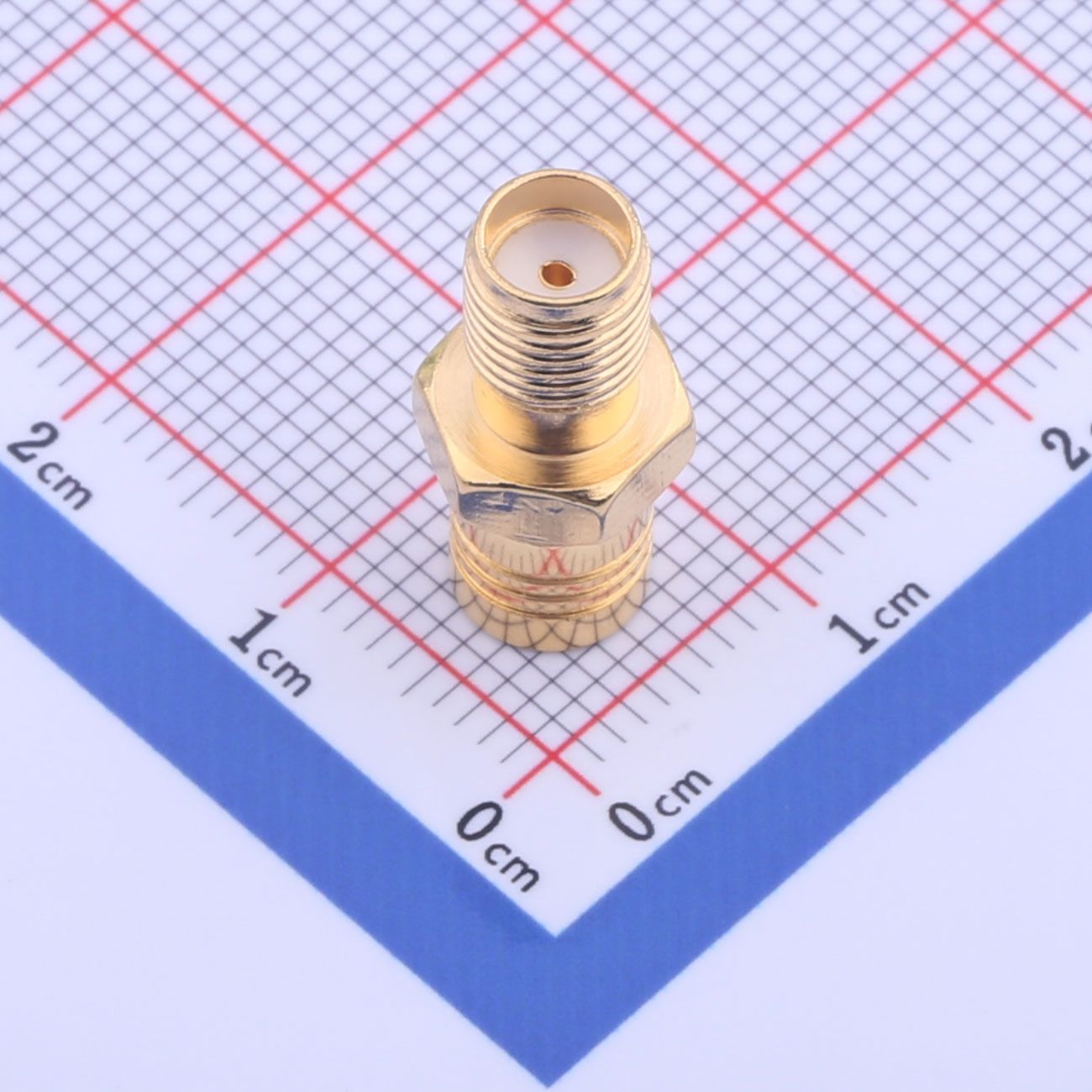
RF Adapter: What It Is, How It Works, and How to Choose the Right One
2026-05-19
231
Core answer: An RF adapter is a passive electrical component that mechanically and electrically connects two RF connectors of different types, genders, or sizes — enabling signal continuity across mismatched interfaces without redesigning the cable or device. If you work with coaxial cables, test equipment, antennas, or wireless systems, understanding RF adapters will save you time, reduce signal loss, and prevent costly compatibility mistakes.
Who this is for: Engineers, technicians, and technically informed buyers who need to interconnect RF components across different connector standards. This article assumes basic familiarity with coaxial cables and connector types.
Who should look elsewhere: If you need to amplify, filter, or condition an RF signal — not just bridge a mechanical mismatch — you need an active component (amplifier, attenuator, or filter), not an adapter.
What Is an RF Adapter?
An RF adapter (also called an RF connector adapter or RF coaxial adapter) is a short, passive coupling device that joins two coaxial connectors that would not otherwise mate directly. It preserves the 50 Ω or 75 Ω impedance of the transmission line, maintains shielding continuity, and introduces only minimal insertion loss when properly specified.
The term covers a broad family:
Type-conversion adapters— connect two different connector standards (e.g., SMA to BNC, N to SMA, TNC to MCX)
Gender-change adapters— connect two connectors of the same type but opposite gender (male-to-female RF adapter, or "barrel" adapters)
In-series adapters— join two connectors of the same type and same gender (less common; used in test bench setups)
What all RF adapters share is a coaxial internal structure: a center pin or socket that carries the signal, surrounded by a dielectric, surrounded by an outer conductor and mechanical interface. This is why the terms "RF coaxial adapter" and "RF adapter" are often used interchangeably in product catalogs.
How the Signal Travels Through an Adapter
The center conductor of the first connector mates with the center conductor of the adapter body, which connects internally to the center conductor of the second interface. The outer shield is continuous through the body. The dielectric material (typically PTFE) maintains the characteristic impedance. Electrically, a well-designed adapter looks like a very short length of matched coaxial line — ideally invisible to the signal.
Performance degrades when:
The adapter's rated frequency ceiling is exceeded (impedance discontinuities become significant at high frequencies)
The dielectric or geometry is compromised by mechanical wear, overtorquing, or contamination
Two adapters are stacked in series, compounding the impedance steps
Common RF Adapter Types and Their Use Cases
SMA to RF Adapter (SMA to Other Standards)
SMA (SubMiniature version A) is one of the most widely used RF connectors in the industry, rated typically to 18 GHz (standard) or up to 26.5 GHz (precision). An SMA to RF adapter commonly bridges SMA to N-type, BNC, TNC, MCX, or MMCX interfaces.
Typical use cases:
Connecting an SMA-terminated cable from a software-defined radio (SDR) to a legacy N-type antenna port
Interfacing SMA-based laboratory instruments with BNC-terminated test cables
Prototyping wireless modules that use MMCX on the PCB to SMA-based bench equipment
Verification tip: Confirm the adapter's upper frequency limit exceeds your highest signal frequency by a comfortable margin (at least 20–30%). For wideband or high-frequency work, check the return loss (VSWR) specification, not just the connector type compatibility.
BNC RF Adapter (RF Adapter BNC)
BNC (Bayonet Neill–Concelman) connectors are rated to 4 GHz (standard) and are ubiquitous in video, baseband, and lower-frequency RF applications. A BNC RF adapter typically appears in:
Test and measurement setups (oscilloscopes, signal generators, spectrum analyzers)
Legacy broadcast and CCTV infrastructure
Bridging BNC-terminated equipment to SMA, N-type, or TNC systems
Because BNC's 4 GHz ceiling is relatively low, using a BNC RF adapter in a microwave application will introduce significant reflection and loss above that limit. This is a common mistake (see the Misconceptions section below).
RF Antenna Adapter
An RF antenna adapter is functionally the same as a general RF coaxial adapter, but the term is typically used in the context of adapting an antenna's connector to the radio or device port. Common scenarios include:
Adapting a vehicle antenna with a DIN or Motorola connector to a device with an SMA port
Connecting a Wi-Fi antenna (RP-SMA) to standard SMA equipment (note: RP-SMA uses a reversed center pin — these are notinterchangeable with standard SMA without the correct adapter)
Bridging an N-type outdoor antenna to an SMA indoor radio module
Critical note on RP-SMA vs. SMA: These look visually similar but are mechanically and electrically incompatible without the correct RF antenna adapter. Forcing an RP-SMA connector onto a standard SMA port will not make proper electrical contact and may damage both parts.
Male to Female RF Adapter
A male-to-female RF adapter (also called a gender changer or barrel adapter) connects two connectors of the same type that both present the same gender. The most common form is female-to-female (joining two male-terminated cables) or male-to-male (joining two female ports, less common).
Where this matters: In test setups where a cable run ends in the wrong gender for the device under test; in panel-mount situations where a bulkhead jack needs to be extended without re-terminating the cable.
Caution: Each adapter in a signal chain adds a small impedance discontinuity and mechanical connection point. In high-frequency or high-reliability installations, minimize the number of stacked adapters. If you regularly need a gender change at a specific point, consider re-terminating the cable with the correct connector type.
RF Signal Adapter vs. RF Adapter Cable
These two terms describe related but distinct products:
RF Signal Adapter
RF Adapter Cable
Form
Compact, rigid body; direct mating
Short flexible cable with two different connectors
Typical length
Near-zero (body length only)
15 cm – 60 cm typically
Flexibility
None — connectors must align
Can route around mechanical obstacles
Loss
Minimal (body only)
Higher (cable length adds attenuation)
Best for
Direct port-to-port in same panel or rack
Misaligned ports, strain relief, awkward angles
An RF adapter cable (also called a pigtail or jumper) is the right choice when two ports cannot physically align for a rigid adapter, or when mechanical stress relief is needed to protect the connector.
Key Specifications to Evaluate When Selecting an RF Adapter
Choosing the wrong adapter is one of the most common causes of unexplained signal degradation in RF systems. Evaluate these parameters before purchasing:
1. Impedance (50 Ω vs. 75 Ω)
Most RF systems operate at either 50 Ω (telecommunications, test equipment, wireless) or 75 Ω (broadcast video, cable TV, CATV). Mixing a 50 Ω adapter into a 75 Ω system (or vice versa) creates an impedance mismatch that reflects signal energy and causes VSWR (Voltage Standing Wave Ratio) degradation.
How to verify: Check the adapter's impedance specification in the datasheet. If the datasheet does not list impedance, treat the adapter as uncharacterized for precision work. Measure VSWR with a network analyzer or return loss bridge if the application is critical.
2. Frequency Range
Every connector type has a maximum usable frequency determined by its physical geometry (the smaller the connector, the higher the cutoff frequency generally extends). A mismatch between the adapter's rated frequency and the signal frequency is a primary cause of signal loss and reflections.
Reference ranges (approximate, per IEEE 287 and connector manufacturer standards):
Connector
Approximate Frequency Limit
N-type
18 GHz (standard)
SMA
18 GHz (standard) / 26.5 GHz (precision)
TNC
11 GHz
BNC
4 GHz
MCX
6 GHz
MMCX
6 GHz
SMP (GPO)
40 GHz
3. Insertion Loss
Insertion loss is the signal power lost as it passes through the adapter, expressed in dB. A well-made, properly specified adapter should contribute less than 0.2–0.3 dB of additional loss at frequencies well below its rated limit. Exceeding the frequency limit or using a low-quality adapter can dramatically increase this.
How to verify: Request the S21 (insertion loss) vs. frequency plot from the manufacturer's datasheet, or measure it with a vector network analyzer (VNA) across your operating band.
4. Power Handling
Adapters have maximum continuous power ratings (typically specified in Watts). Exceeding this causes dielectric heating, potential arcing, and connector failure. This matters primarily in transmit paths (base stations, amplifier outputs, radar).
5. Mechanical Durability (Mating Cycles)
Standard commercial RF adapters are typically rated for 500–1,000 mating cycles. Precision adapters (used in test equipment) may be rated to 5,000+ cycles. In high-cycle environments (automated test, frequent reconfiguration), specify accordingly.
How to Install and Inspect an RF Adapter Correctly
Improper installation is a leading cause of premature connector failure and signal integrity problems.
Quick check before mating:
Inspect both connectors for bent center pins, debris, or corrosion
Verify gender and type compatibility
Confirm the adapter's rated frequency and impedance match the system
Steps:
Align the connector interfaces — do not force or cross-thread
Hand-tighten first to confirm smooth thread engagement
Torque to the manufacturer's specified value using a calibrated torque wrench (common values: SMA = 0.9 N·m / 8 in-lb; N-type = 1.36 N·m / 12 in-lb; BNC = finger-tight only for bayonet)
Do not over-torque — this deforms the center contact and dielectric
Verify after installation:
Visually inspect for center pin alignment and flush seating
Measure VSWR or return loss at the system operating frequency if equipment permits
For critical links, measure insertion loss before and after to confirm the adapter contribution is within spec
Failure signals:
Higher-than-expected noise floor or attenuation in the system
Intermittent signal dropout under vibration or temperature change
Visible damage: scored threads, deformed center pin, cracked dielectric
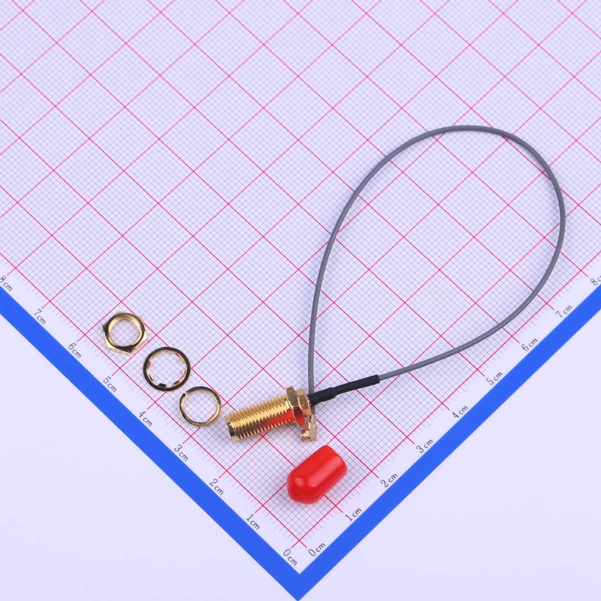
What Is RF Cable Assembly and How Does It Work?
2026-05-12
326
An RF cable assembly is a ready-to-install transmission line: one or more coaxial cables cut to a defined length and terminated at each end with RF connectors, enabling radio frequency signals to travel between system components with controlled impedance, low signal loss, and effective electromagnetic shielding.
This guide is for electronics engineers, hardware designers, procurement engineers, and technical buyers who need to evaluate, specify, or source RF cable assemblies for wireless, automotive, or industrial RF systems.
This guide does not replace application-specific RF link budget simulation, compliance testing, or regulatory certification. For regulated transmitter systems, verify your cable assembly selection against applicable EMC and RF emissions standards in your target market.
Why the Assembly Matters More Than the Cable Alone
RF cable assemblies are frequently treated as commodity parts — ordered by length and connector label — but an incorrectly specified assembly degrades system performance in ways that are difficult to isolate during troubleshooting.
Consider: a cable with 3 dB insertion loss wastes half of the available signal power before it reaches the antenna. At frequencies above 3 GHz, even connector plating thickness, contact geometry, and cable bending radius affect measurable performance. The connector-to-cable transition is typically the highest-variability point in the assembly, and it is where most quality problems originate.
The five decisions this guide covers — cable construction, characteristic impedance, connector interface, environmental rating, and assembly quality criteria — each map to a specific, measurable RF parameter. The relevant verification method is included in each section.
What Is a Cable Assembly in RF Systems?
What is a cable assembly, precisely? In any electrical context, a cable assembly is a cable that has been:
Cut to a specified length
Prepared at each end (stripped, cleaned, soldered or crimped)
Fitted with connectors, making it installable without field modification
In RF systems, a cable assembly radio frequency product must accomplish two simultaneous goals:
Transmit signal — guide electromagnetic energy from source to load
Contain signal — prevent the cable from radiating outward (causing EMI interference to adjacent systems) or from absorbing external interference (adding noise)
Both goals are achieved by the coaxial construction described in the next section.
Anatomy of a typical RF coaxial cable assembly:
Component
Role
Center conductor
Carries the RF signal current
Dielectric insulator
Maintains precise conductor spacing; controls impedance
Outer conductor (braid or foil)
Provides the return current path and EM shielding
Jacket
Mechanical and environmental protection
Connectors (×1 or ×2)
Interface with system ports; must maintain impedance continuity at the transition
Applicable standards include IEC 61169 (RF connector dimensions and performance), MIL-DTL-17 (U.S. military coaxial cable specifications), and IEC 62153 (RF cable measurement methods). These define the dimensional tolerances, insertion loss limits, and test procedures that qualified suppliers reference.
How RF Cable Works: Signal Propagation in a Coaxial Structure
Understanding how RF cable works at a structural level lets you predict where problems occur and what test data to request.
The Coaxial Principle
In a coaxial cable, the electromagnetic field carrying the RF signal exists entirely in the dielectric region between the center conductor and the outer conductor. The outer conductor acts as both the return current path and a Faraday shield — the signal is geometrically self-contained, which is why coaxial cables outperform open-wire lines for RF signal transmission in interference-dense environments.
Characteristic Impedance (Z₀)
Impedance is set by the geometry and dielectric material — specifically by the ratio of conductor diameters and the dielectric constant (εr) of the insulator:
Z₀ = (138 / √εr) × log₁₀(D/d)
Where D = inner diameter of the outer conductor, d = outer diameter of the center conductor.
Nearly all RF communications systems are designed for 50 Ω impedance. Broadcast video and cable TV systems use 75 Ω. If a cable assembly's impedance does not match the system at both ends, signal reflections occur — measured as VSWR (Voltage Standing Wave Ratio). A VSWR of 1.0:1 is ideal. Values above 2.0:1 indicate a mismatch significant enough to affect link performance.
How to verify: A vector network analyzer (VNA) measures S11 (return loss) and derives VSWR directly. For procurement validation, ask your supplier whether cable assemblies are 100% swept-tested and request sample test reports showing VSWR across your operating band, not at a single frequency.
Signal Attenuation (Insertion Loss)
Every cable loses some signal to resistive losses in the conductors and dielectric absorption. Attenuation increases with:
Higher frequency (conductor losses scale approximately with √frequency)
Longer physical length
Smaller cable diameter
Higher dielectric constant (solid polyethylene has higher loss than foamed or air-spaced PTFE)
How to verify: Request the attenuation curve (dB per 100 feet or dB per meter) across your full operating frequency range. Use it to calculate total insertion loss for your cable run. Single-frequency datasheets are insufficient for wideband systems.
Frequency Limits
Every coaxial cable has a maximum operating frequency above which higher-order propagation modes appear and signal integrity degrades. This cutoff is determined by the dielectric diameter. Thin cables used with IPEX/MHF connectors (≈1.13 mm outer diameter) are typically rated to 6 GHz. Larger-format cables (RG-8, LMR-400 equivalents) may be rated to 2–3 GHz but offer substantially lower attenuation within that range.
Connector Types: SMA, IPEX, FAKRA, N-Type, DIN, and MCX
The connector is the mechanically most vulnerable component in any RF cable assembly, and it defines frequency range, mating durability, and system compatibility.
SMA (SubMiniature version A)
The SMA RF cable assembly is the reference choice for laboratory, microwave, and general RF applications. SMA connectors operate to 18 GHz (precision versions to 26.5 GHz), use threaded coupling for secure mating, and are specified at 50 Ω.
Use for: test equipment ports, filters, amplifiers, PCB RF connectors, antenna test benches
Mating cycle life: typically 500+ cycles per IPC/WHMA-A-620 cable harness standards
Avoid for: tool-free quick-connect applications; automotive environments without additional vibration retention hardware
Note: RP-SMA (Reverse Polarity SMA) connectors look identical to standard SMA but have the center pin and socket reversed. They mate mechanically but pass no signal. Check the part number explicitly if your equipment uses RP-SMA (common in consumer Wi-Fi routers).
IPEX / MHF (U.FL Compatible)
The IPEX cable assembly uses a surface-mount, snap-on micro connector — the dominant board-level RF interface in smartphones, laptop Wi-Fi modules, and embedded IoT modules where PCB space is the primary constraint.
Frequency rating: IPEX MHF1 to 6 GHz; MHF4 variants to 10 GHz
Mating cycle life: approximately 30 cycles — treated as a design-time connection, not a field-serviceable one
Use for: PCB-to-antenna routing in compact consumer and industrial electronics
Three common pigtail configurations:
Configuration
Application
IPEX to SMA cable assembly
Connects a board-level IPEX port to an SMA test port or panel-mount antenna
IPEX to IPEX cable assembly
Routes signal between two board-level IPEX ports inside the same enclosure
IPEX to soldering RF cable
Bare-wire termination for direct solder to a PCB pad where no mating connector footprint is available
FAKRA (DIN 72594-1 Automotive RF Connector)
The FAKRA cable assembly is the automotive-grade RF connector defined by the DIN 72594-1 standard. Color-coded, keyed housings prevent incorrect mating — essential on vehicle assembly lines where GPS, AM/FM, DAB, cellular, and V2X antenna connections are routed simultaneously.
Use for: vehicle antenna feeds — GPS, DAB/AM/FM, cellular (4G/5G), V2X, ADAS radar connections
Key advantage: positive keying prevents miswiring regardless of operator attention level; sealed variants rated for under-hood environments
Frequency: rated to approximately 3 GHz for standard FAKRA; FAKRA Mini (HSD) variants support higher data-rate automotive applications
Common automotive RF cable assembly configurations using FAKRA:
Configuration
Typical Use
FAKRA to FAKRA cable assembly
Antenna extension or body harness-to-module connection within the vehicle
IPEX to FAKRA cable assembly
Board-level module to vehicle antenna harness interface
BNC to IPEX cable assembly
Development bench to compact automotive module; BNC is common on signal generators and spectrum analyzers
N-Type
The N Type RF Cable Assembly uses a medium-sized, threaded connector rated to 11 GHz (18 GHz for precision variants). Its larger contact area supports higher power levels than SMA, and its mechanical construction withstands outdoor and industrial environments.
Use for: base station feedlines, outdoor antenna mounts, high-power RF amplifiers, satellite ground equipment
Power handling: significantly higher than SMA at equivalent frequencies
Critical warning: 50 Ω and 75 Ω N connectors are dimensionally nearly identical but electrically incompatible. Confirm impedance designation on both sides before connecting.
DIN 7-16
The DIN RF Cable Assembly uses the 7-16 DIN connector (the modern 4.3/10 is a compact variant), a large-format interface found in cellular base stations and distributed antenna systems (DAS).
Use for: high-power base station interconnects, DAS nodes, tower-mounted amplifiers
Key property: exceptionally low passive intermodulation distortion (PIM), which is critical in multi-carrier cellular systems where intermodulation products fall within receive bands
SMA to MCX
SMA to MCX cable assembly adapts SMA to the compact, snap-on MCX connector used in GPS receivers, compact RF modules, and automotive telematics units. MCX is rated to 6 GHz and uses the same 50 Ω impedance.
How to Select the Right RF Cable Assembly
Work through these steps in order. Each narrows your viable options.
Step 1 — Define frequency range and loss budget
Identify the highest operating frequency in your system and the maximum allowable insertion loss for the cable run. At your target frequency, use the manufacturer's published attenuation table to calculate whether a given cable type meets your loss budget over the required length. For runs longer than 1–2 meters above 2 GHz, evaluate a low loss RF cable assembly using foam or air-spaced PTFE dielectrics — these can offer 2–5× lower attenuation per meter compared to standard solid-PE cables of the same outer diameter.
How to verify: Request attenuation data across your full operating band, not a single-frequency figure. For a field-installed run, measure insertion loss end-to-end with a calibrated source and power meter or a VNA after installation.
Step 2 — Confirm impedance on both sides
Confirm that the cable impedance matches both interface ports. 50 Ω for RF communications; 75 Ω for broadcast/CATV. Mismatched impedance creates reflections that increase VSWR and reduce effective signal transfer regardless of how good the cable itself is.
Step 3 — Select connector interface
Match connectors to your equipment ports using the connector reference above. If you need to bridge two different connector families, use a single adapter cable rather than stacking mechanical adapters — each adapter-to-adapter interface is an additional loss and mechanical failure point.
Step 4 — Specify environmental conditions
Environment
Cable/Connector Selection
Indoor lab
Standard PVC jacket; SMA, BNC, or MCX
Outdoor exposed
UV-stabilized jacket; sealed N-type or weatherproof SMA; self-amalgamating tape or weatherproof boots on field joints
Automotive
FAKRA or FAKRA Mini; operating temperature typically −40 °C to +85 °C or higher; vibration-rated crimp termination
High-power RF
N-type or DIN 7-16; confirm power derating curve vs. frequency before specifying
Step 5 — Verify assembly quality before accepting
Before accepting production-quantity RF cable assemblies from any supplier:
Request 100% electrical test data (swept return loss and insertion loss) — not batch sample testing
Confirm connector plating specification: gold-plated contacts maintain contact resistance over mating cycles and resist corrosion
Review VSWR specification across the full operating band
For safety-critical or certification-required applications, request a Certificate of Conformance (CoC) and raw material lot traceability
Antenna Cable Assembly: The Feedline as a System Element
The antenna cable assembly — the feedline connecting an antenna to a receiver or transmitter — is one of the most performance-critical placements in any RF system. Every decibel lost in the feedline either increases the required transmit power or degrades receiver sensitivity.
Principles for antenna feedlines:
Minimize cable length wherever installation geometry permits. In receive-critical systems, mount a low-noise amplifier (LNA) as close to the antenna as possible, before the cable run, rather than at the receiver end.
Seal all outdoor connections. Moisture ingress at an improperly sealed N-type or FAKRA joint causes galvanic corrosion at the contact interface. The resulting insertion loss increase is gradual, difficult to notice without baseline measurements, and significant over months to years of outdoor exposure.
Confirm power rating at operating frequency. Power handling capacity for coaxial cables decreases with frequency. The same cable rated at 100 W at 30 MHz may be rated at 20 W at 3 GHz. Always check the derating curve at your carrier frequency, not just the peak headline power figure.

RF Connector Guide: Types, Selection Criteria, and Applications
2026-05-06
681
Core answer: An RF connector is a precision electromechanical interface that transfers radio-frequency signals between cables, PCBs, and antennas with controlled impedance and minimal signal loss. Choosing the wrong type—or the right type but with mismatched impedance—causes reflections, insertion loss, and system-level failures that are difficult to trace after assembly.
Who this guide is for: Electronics engineers, RF system designers, and technical procurement teams who need to specify, evaluate, or compare RF connectors for a project. If you are entirely new to RF concepts, you may want to review basic transmission-line theory first; if you are already specifying connectors daily, this guide offers a consolidated decision framework and a checklist of the most common specification errors.
Who this guide is not for: Individuals looking solely for consumer-grade installation guidance; the connector families covered here are oriented toward RF/microwave engineering contexts.
What Is an RF Connector and Why Controlled Impedance Matters
An RF connector is not simply a plug and socket. At radio frequencies—typically from a few MHz into the tens of GHz—signal wavelengths become short relative to the physical dimensions of your circuit. Any discontinuity in the transmission path (a connector with the wrong geometry, a mismatched impedance, an air gap from mechanical wear) creates a reflection. That reflection travels back toward the source, reduces delivered power, and can distort the signal. The ratio of reflected to incident power is quantified as the Voltage Standing Wave Ratio (VSWR) or, equivalently, as return loss in dB.
RF connector impedance is the single most consequential specification. The two standard impedance values are:
50 Ω– The dominant standard for RF and microwave work: test equipment, antennas, cellular infrastructure, Wi-Fi, radar, and laboratory instrumentation. The 50 Ω value represents a historical compromise between minimum loss (~77 Ω for air-dielectric coax) and maximum power handling (~30 Ω), and it is codified in IEC 61169 and related standards.
75 Ω– Standard for video broadcast, cable television (CATV), and satellite distribution, where long-cable signal-to-noise ratio is prioritized over power delivery. Mixing 50 Ω and 75 Ω connectors in the same signal path is a frequent and costly error—detailed further in the selection framework below.
How to verify impedance compliance: A vector network analyzer (VNA) measuring S11 (return loss) at the connector interface is the definitive method. A return loss better than −20 dB (VSWR < 1.22:1) across your operating band is a commonly accepted threshold for low-reflection connectors, though your system budget may be tighter. Time-domain reflectometry (TDR) can also localize impedance discontinuities to a specific connector or cable segment. If you do not have lab access, the connector's published datasheet—cross-checked against IEC 61169 series sub-part specifications—is the appropriate verification path.
RF Connector Types: A Practical Overview
The table below summarizes the connector families covered in this guide. Frequency ratings are typical maximums for the standard connector body; precision variants of the same interface can sometimes exceed these values. Always verify against the specific part datasheet.
Connector
Impedance
Typical Max Frequency
Coupling
Primary Use Case
SMA
50 Ω
18 GHz (standard); up to 26.5 GHz (precision)
Threaded (5/16-32 UNS)
Lab instruments, Wi-Fi, LTE modules, PCB
BNC
50 Ω / 75 Ω
~4 GHz
Bayonet (quarter-turn)
Test equipment, video, legacy comms
Type N
50 Ω / 75 Ω
~11–18 GHz
Threaded
Outdoor antennas, base stations, high-power
TNC
50 Ω
~12 GHz
Threaded
Mobile/portable RF, moderate vibration
MCX / MMCX
50 Ω
~6 GHz
Snap-on / threaded micro
GPS, compact wireless modules, PCB
U.FL (IPEX)
50 Ω
~6 GHz
Snap-on (board-mount)
Consumer electronics, IoT, laptop Wi-Fi
This rf connector types chart reflects general industry positioning; specific datasheets from connector manufacturers govern binding specifications.
RF Connector SMA
The Sub-Miniature version A (SMA) connector is the workhorse of the RF and microwave industry. Its 3.5 mm inner-contact diameter and threaded coupling mechanism deliver a reliable, repeatable connection up to approximately 18 GHz for standard versions—and up to 26.5 GHz for precision SMA variants that maintain tighter mechanical tolerances.
Key characteristics:
50 Ω impedance; PTFE dielectric is standard
Rated torque: typically 0.45–0.56 N·m (4–5 in-lb) for the coupling nut—overtightening is a leading cause of field failures
Available in edge-mount, end-launch, surface-mount, and through-hole configurations for RF connector PCBintegration
Reverse-polarity SMA (RP-SMA) uses a reversed center-pin convention and is notinteroperable with standard SMA; confirming polarity at procurement is a critical step
When to choose SMA: Any application operating below 18 GHz that requires a compact, widely sourced threaded interface. The SMA ecosystem—cables, adapters, attenuators, calibration standards—is the most mature in the industry.
When to look elsewhere: Above 18 GHz, consider the 2.92 mm (K) or 2.4 mm connector, which are backward-compatible with SMA mechanically but maintain full specification to higher frequencies.
RF Connector BNC
The Bayonet Neill–Concelman (BNC) connector is characterized by its quarter-turn bayonet locking mechanism, making it fast to connect and disconnect. Its practical upper frequency limit is approximately 4 GHz for the 50 Ω variant.
Key characteristics:
Available in both 50 Ω (general RF/test) and 75 Ω (video/broadcast) versions
The physical interface is dimensionally identical between 50 Ω and 75 Ω versions—they will mate—but the impedance mismatch degrades performance, particularly above ~1 GHz
Widely used in oscilloscope inputs, signal generators, video equipment, and legacy RF test setups
Lower frequency limit is DC, making BNC suitable for baseband as well as RF signals
When to choose BNC: Test and measurement setups where rapid connection cycling is required, video signal distribution (75 Ω variant), and any application below ~1 GHz where the bayonet convenience outweighs the size and frequency limitations.
RF Connector Type N
The Type N connector was designed for more demanding outdoor and high-power environments than SMA or BNC. Its larger form factor provides robust performance where smaller connectors would be unsuitable.
Key characteristics:
Weatherproofing:The threaded coupling and gasket-sealed interface make Type N suitable for outdoor antenna installations and base-station equipment
Higher power handling:Typically several hundred watts continuous at lower frequencies, versus tens of watts for SMA
Frequency range:Standard 50 Ω Type N to ~11 GHz; precision versions to ~18 GHz
75 Ω variants exist for CATV infrastructure, but the 50 Ω version represents the majority in RF/microwave engineering
When to choose Type N: Outdoor antenna feeds, cellular base-station cabling, high-power amplifier outputs, and anywhere the connector must survive environmental exposure or mechanical stress over years of service.
RF Connector TNC
The Threaded Neill–Concelman (TNC) connector is essentially a BNC with a threaded coupling mechanism instead of a bayonet. That single change improves performance at higher frequencies (up to ~12 GHz) and provides better resistance to vibration—making TNC the preferred choice for portable and vehicle-mounted radio equipment.
Key characteristics:
50 Ω impedance; threaded interface prevents accidental disconnection under vibration
Electrically superior to BNC above ~1–2 GHz due to the more consistent mating geometry enabled by threading
Common in handheld radio transceivers, GPS antennas, and mobile communications infrastructure
When to choose TNC over BNC: Applications above ~1–2 GHz, or any environment with mechanical vibration that could cause a bayonet connection to disengage.
MCX, MMCX, and U.FL: Compact Board-Level Connectors
For space-constrained PCB applications—GPS receivers, Wi-Fi modules, IoT devices—miniature connectors dominate.
MCX:Snap-on coupling, ~6 GHz, larger than MMCX; used in automotive and compact wireless assemblies
MMCX:Threaded micro interface, ~6 GHz, very small footprint; common on module-to-cable transitions
FL (also marketed as IPEXor MHF): Ultra-compact snap-on board-mount connector, ~6 GHz; rated for approximately 30 mating cycles—appropriate for semi-permanent connections, not frequently cycled test interfaces
These connectors are almost always used in conjunction with a pigtail cable assembly that transitions to a larger-format connector (SMA, TNC, Type N) at the panel or antenna interface.
How to Select the Right RF Connector: A Decision Framework
Selecting an rf connector requires answering six questions in order. Skipping any of them is the primary cause of rework and system-level failures.
What is your system impedance?Establish this first. Most RF/microwave systems are 50 Ω. Every connector in the signal chain must match. Do not mix 50 Ω and 75 Ω interfaces; the physical compatibility of some connector families (BNC, Type N) does not imply electrical compatibility, and the resulting mismatch loss (~0.18 dB insertion loss, ~−14 dB return loss at the junction) will degrade system performance.
What is your maximum operating frequency?Add margin: if your signal occupies 0–6 GHz, a connector rated to 6 GHz leaves no headroom for harmonics or future expansion. A connector rated to 12 GHz or 18 GHz in that slot is prudent.
What is your power level?Connector datasheets specify peak and average power ratings. Exceeding these causes dielectric breakdown or thermal damage. Type N and 7/16 DIN connectors support higher power levels than SMA or BNC.
What is the mechanical interface requirement?
PCB mount:Surface-mount edge-launch, end-launch, or through-hole? Board thickness and dielectric constant affect which end-launch configuration maintains 50 Ω through the transition.
Cable termination:What cable family? A connector specified for RG-316 is not dimensionally compatible with RG-58.
Coupling mechanism:Threaded (SMA, Type N, TNC) for permanence and high-frequency integrity; bayonet (BNC) for rapid cycling; snap-on (U.FL, MCX) for compact board assemblies with low cycle counts.
What are the environmental requirements?Outdoor, high-vibration, or high-humidity environments require connectors with environmental sealing (IP rating) and appropriate coupling torque retention. Type N and ruggedized TNC are designed for these conditions; standard SMA is not.
What is your source for the connector or cable assembly?For rf cable assemblies, the connector body, the cable, and the termination method must be specified together. A precision SMA connector terminated incorrectly—wrong strip length, center-pin protrusion out of tolerance—will underperform a standard connector terminated correctly. Review the manufacturer's assembly drawings and, where possible, request test data (insertion loss, VSWR) on production samples.
RF Connectors on PCBs and in Cable Assemblies
PCB-Mount RF Connectors
Integrating an rf connector pcb interface is one of the most common points of signal integrity failure in hardware design. The transition from the connector's internal geometry to the PCB microstrip or stripline creates an impedance discontinuity unless the PCB footprint is designed to compensate.
Key design considerations:
Use the connector manufacturer's recommended land pattern and board-stack specification (dielectric constant, trace width, ground clearance)
Via-in-pad placement and ground pour management under the connector body affect the reference plane continuity; validate with EM simulation before final layout
Edge-launch connectors require tight control of board edge quality; rough edges increase the effective transition length and degrade high-frequency performance
FL and MMCX connectors are appropriate for semi-permanent connections, not frequently cycled test interfaces, given their limited mating cycle ratings
RF Cable Assemblies
RF cable assemblies combine a cable (defined by its characteristic impedance, dielectric type, outer diameter, and loss-per-length) with connectors at each end, terminated to a specific assembly drawing. The total insertion loss of an assembly is the sum of connector insertion loss plus cable attenuation—both are frequency-dependent and increase with frequency.
When specifying cable assemblies, verify:
Cable type (e.g., RG-316, LMR-400, phase-stable low-loss types) and its loss specification at your maximum frequency
Connector type at each end—assemblies with mixed connector families (SMA to Type N, BNC to SMA) are common and should be explicitly specified in the purchase order
VSWR across the full operating band, not just at a single frequency point
Environmental rating if the assembly will be routed outdoors or in industrial environments
Phase stability under temperature and flexure, if your application is phase-sensitive (antenna arrays, phased-array radar, test equipment calibration)
Summary: Selecting RF Connectors Without Rework
The rf connector guide above reduces to five decision rules:
Lock your impedance standard first.50 Ω and 75 Ω are not interchangeable, even when the physical interfaces mate.
Add frequency headroom.Specify a connector rated to at least 1.5× your maximum operating frequency.
Match the connector to the environment.Outdoor, high-power, or high-vibration environments require Type N or ruggedized TNC—not standard SMA.
Specify the PCB footprint alongside the connector.The transition from connector to board trace is where most PCB-level return loss problems originate.
Treat cable assemblies as a system.Cable type, connector type, termination method, and acceptance test criteria must all be specified in the same document.
For a consolidated view across all connector families, the rf connector types chart in the overview section above provides a starting reference; always validate against manufacturer datasheets for the specific part under consideration.
RF Antenna Design: A Practical Guide for Intermediate Engineers
2026-04-28
941
The Short Answer
If you understand transmission-line theory and can calculate a quarter-wave length, you already have the foundation to design a functional RF antenna. This guide is for embedded engineers, hardware designers, and IoT developers who need a working antenna—not an antenna specialist who needs a production-grade phased array. If you are designing a high-gain multi-element array for aerospace or 5G base-station work, you need electromagnetic simulation software and specialist review beyond what this article covers.
RF Antenna Basics: What You Must Understand First
An antenna converts a guided electromagnetic wave (traveling along a transmission line or PCB trace) into a free-space radiated wave, and vice versa. Three parameters govern almost every design decision:
1. Resonant frequency. An antenna is most efficient when its physical length relates to the wavelength (λ) of the target frequency. The free-space wavelength is:
λ (meters) = 300 / f (MHz)
At 2.4 GHz, λ ≈ 125 mm. At 868 MHz (LoRa EU), λ ≈ 345 mm.
2. Impedance. Most RF systems are designed for 50 Ω characteristic impedance. A mismatch between the antenna and the feed line causes reflections, measured as return loss (S11) or VSWR. A good target is S11 < −10 dB (VSWR < 2:1), meaning less than 10% of power is reflected.
3. Radiation pattern. A simple monopole or dipole radiates omni-directionally in the horizontal plane—suitable for most IoT use cases. Directional gain (patch, Yagi) trades coverage angle for range.
RF Antenna Length: How to Calculate It
Quarter-wave monopole is the most common starting point. Its free-space length is:
L = λ / 4 = 75 / f (MHz) [meters]
Frequency
Free-space λ/4
433 MHz
173 mm
868 MHz
86.4 mm
915 MHz
82.1 mm
2.4 GHz
31.2 mm
Velocity factor correction: When the antenna is implemented as a PCB trace or wire near a dielectric, the effective wavelength shortens. A common empirical correction factor for FR4 PCB traces is 0.97–0.95 (close to free space for a wire antenna above the board). For a meandered or ceramic chip antenna, the manufacturer's datasheet provides the effective length or a pre-matched design—use it directly.
How to verify: Measure S11 with a vector network analyzer (VNA) or a low-cost NanoVNA. Tune physical length ±5–10% around the calculated value and look for the S11 dip at your target frequency. This is the single most reliable verification step.
RF Antenna Matching: Fixing Impedance Mismatches
Most antenna failures in real products trace back to impedance mismatch—not antenna geometry. Here is a practical matching workflow:
Quick-Check → Steps → Verify → Common Failures
Quick check: Measure S11 at the antenna feed point before adding any matching components. If S11 < −10 dB at your target frequency, the antenna is already acceptable—stop here.
Steps (L-network matching):
1. Identify the impedance at the feed point from VNA data (real + imaginary parts, e.g., 35 − j20 Ω).
2. Use an online Smith chart tool or a calculator (e.g., TCCQ, SimSmith) to find an L-network that transforms that impedance to 50 Ω.
3. Place a shunt capacitor and series inductor (or the reverse, depending on the quadrant) using 0402 or 0201 SMD components with tight tolerances (±1–2%).
4. Start with calculated values; sweep ±20% in the BOM to account for component parasitics.
Verify: Re-measure S11 after placing matching components. Target: S11 ≤ −10 dB, ideally ≤ −15 dB, across the operating channel bandwidth.
Common failures:
PCB land patterns for 0402 components introduce ~0.5–1 nH parasitic inductance. Account for this in simulation or iterate with VNA.
Solder joints add parasitic capacitance; reflow quality matters.
Matching at the bench may shift in a plastic enclosure. Always re-verify in the final mechanical assembly.
RF PCB Antenna Design: Layout Rules That Actually Matter
PCB antenna performance is heavily influenced by layout, not just schematic. Follow these rules for FR4 two-layer boards (the most common IoT scenario):
1. Clearance zone (keep-out area). The antenna radiating element needs a copper-free zone beneath and around it. For a 2.4 GHz PCB trace antenna, a minimum 3–5 mm keep-out from the ground plane is typical.
2. Ground plane size affects resonance. A quarter-wave monopole requires a ground plane to radiate efficiently. If the ground plane is smaller than λ/4, the effective frequency shifts.
3. Feed-line routing. Route the 50 Ω microstrip feed line as short as possible between the RF IC/module and the antenna feed point.
4. Isolation from noisy components. Keep switching regulators, crystal oscillators, and high-speed digital buses at least 5–10 mm away from the antenna and RF feed path.
5. Pi-network footprint. Always place a pi-network (three pads: shunt-series-shunt) on the feed path even if populated with 0 Ω / open initially.
How to Design an RF Antenna: Step-by-Step Summary
Prerequisites: Target frequency, PCB stack-up datasheet, a VNA (or access to one), and a reference design or datasheet from the RF IC vendor.
1. Define specs: Frequency, bandwidth, required VSWR, gain, form factor, and regulatory band.
2. Choose antenna type: Wire monopole, PCB trace antenna, or chip antenna.
3. Calculate initial length using the λ/4 formula.
4. Design PCB layout with keep-out zone and pi-network footprint.
5. Populate and measure: Use a VNA to measure S11.
6. Validate in enclosure: Re-measure inside the final housing.
7. Regulatory pre-compliance check: Conduct a pre-scan before final production.
Ready to Source Antennas or RF Connectors for Your Design?
If you are moving from design to hardware, Kinghelm (kinghelm.net) offers a range of RF antennas, connectors, and related components—including options suited to IoT, LoRa, 2.4 GHz Wi-Fi/Bluetooth, and cellular applications.
Sources
1. FCC 47 CFR Part 15 – Radio Frequency Devices
2. EU Radio Equipment Directive (RED)
3. NanoVNA – Open-source VNA project
4. KiCad PCB Impedance Calculator
5. SimSmith – Smith Chart Matching Tool
RF Cable Explained: Understanding RF Cables, Coaxial Cables, RF Jumper Cables, and Assemblies for Reliable Signal Transmission
2026-04-14
904
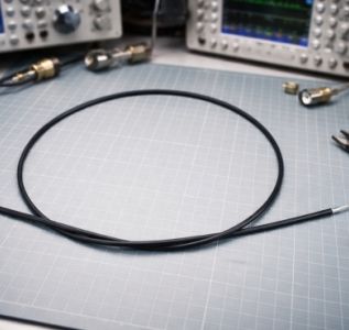
RF cables — also known as coaxial cables, RF coax cables, RF jumper cables, coax jumper cables, or RF cable assemblies when pre-terminated — are specialized transmission lines engineered to carry radio-frequency (RF) signals with high efficiency, low loss, and strong immunity to external interference.
For intermediate engineers, technicians, and system integrators in RF design or maintenance, mastering RF cables means making informed choices that preserve signal integrity from antenna feeds to test equipment or base-station connections. These cables are ideal for applications where controlled impedance, predictable attenuation, and effective shielding are non-negotiable. They are not the best choice for low-frequency power distribution, standard Ethernet data links (better served by twisted-pair), or environments where extreme flexibility without performance trade-offs is required.
What Is an RF Cable and How Does It Differ from General Coaxial Cable?
An RF cable uses the classic coaxial structure: a central conductor, dielectric insulator, concentric outer shield, and protective jacket. The term "RF cable" emphasizes optimization for radio-frequency signals (typically from kHz to GHz), where electromagnetic fields are tightly confined between the inner and outer conductors.
While all RF cables are coaxial, not every coaxial cable is optimized for RF. General-purpose coax (e.g., some video or CATV cables) may use 75 Ω impedance and higher-loss dielectrics suited to lower frequencies, whereas RF-focused cables prioritize 50 Ω impedance, lower attenuation at microwave frequencies, and superior shielding effectiveness. RF jumper cables and coax jumper cables are simply short, flexible segments of these cables, usually fitted with connectors on both ends for quick interconnections between components. RF cable assemblies are factory-terminated versions ready for plug-and-play deployment.
Core Principles: Impedance, Attenuation, and Signal Integrity
The performance of any RF cable rests on three interrelated principles derived from its geometry and materials.
Most RF systems use 50 Ω for a balance of power handling and low attenuation; 75 Ω appears in broadcast and video applications. Mismatched impedance creates reflections, measured as high VSWR (voltage standing wave ratio), which wastes power and can damage transmitters.
Attenuation (signal loss in dB per unit length) rises with frequency due to conductor resistance (skin effect) and dielectric losses. Larger-diameter cables or low-loss dielectrics (foam polyethylene, PTFE, or air-spaced designs) reduce it, but every extra meter or GHz adds measurable degradation.
Shielding effectiveness prevents both radiation of the signal and pickup of external EMI. High braid coverage or foil-plus-braid ("quad shield") constructions deliver better isolation in noisy environments.
RF Jumper Cables and Cable Assemblies in Real-World Use
RF jumper cables excel in short-run connections — for example, linking a base-station radio to an antenna, a filter to a duplexer, or test equipment to a device under test. Their flexibility and pre-installed connectors (SMA, N-type, 4.3-10, etc.) make them practical where rigid lines would be cumbersome.
RF cable assemblies extend this concept with custom lengths, connector types, and sometimes strain-relief boots or armor for harsh conditions. In 4G/5G deployments, telecom towers, satellite ground stations, or lab benches, these ready-made solutions reduce installation time while maintaining consistent electrical performance.
How to Choose the Right RF Cable
Match the cable to your specific requirements:
· Frequency range: Confirm the cable’s rated upper frequency exceeds your operating band.
· Attenuation budget: Calculate total loss using manufacturer charts (dB/m at your frequency × length) and add connector losses.
· Impedance and power handling: Stay within the system’s 50/75 Ω standard and voltage/power ratings.
· Environmental factors: select UV-resistant jackets for outdoor use, low-smoke zero-halogen for plenum spaces, or ruggedized options for vibration.
· Connectors and length: Minimize length to reduce loss; choose mating connectors that maintain impedance continuity.
Always verify against the supplier’s datasheet rather than assuming "standard" performance.
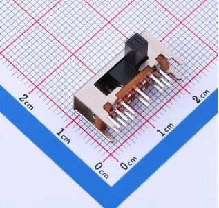
What Is a Slide Switch?
2026-04-07
953
A slide switch is a compact electromechanical component that controls electrical circuits through a simple linear sliding motion. By moving a small actuator (lever or button) along a track, it opens or closes contacts to allow or interrupt current flow. Unlike momentary switches that spring back, a slide switch is a maintained-contact device — it stays in its last position until you deliberately slide it again. This makes it ideal for stable on/off or mode-selection tasks in space-constrained designs.
For intermediate users working on PCBs, prototypes, or consumer electronics, understanding slide switches (often implemented as miniature switches or SPDT variants) means better component selection, fewer field failures, and more intuitive user interfaces. They are not suited for high-current or harsh-environment applications without proper ratings, but excel in low-power, low-voltage scenarios where visual confirmation of state is valuable.
How Slide Switches Work: Basic Principles and Mechanism
Inside a typical slide switch, a conductive slider (wiper) moves across fixed contacts. When you slide the actuator, the wiper bridges or separates the terminals, changing the circuit state. Most designs use gold or silver-plated contacts for low resistance and reliable operation over thousands of cycles.
The linear action provides tactile and visual feedback — you can see and feel the position — which reduces accidental toggling compared to some pushbutton designs. Common electrical ratings range from low-signal levels (a few mA at 5 V) up to moderate loads (several amps at 125 V), depending on the model. Always verify these against your circuit requirements to prevent overheating or contact welding.
To verify a slide switch in your design, use a multimeter in continuity mode: slide the actuator and confirm the expected open/closed states between terminals. This quick L1 check works on any bench and reveals wiring errors or faulty units immediately.
Main Types of Slide Switches: SPST, SPDT, and Beyond
Slide switches come in standard pole-and-throw configurations familiar to anyone using electronic components:
· SPST (Single Pole, Single Throw): Simplest on/off control with two terminals. Use when you only need basic power switching.
· SPDT (Single Pole, Double Throw): Three terminals; routes a single input to one of two outputs. Popular for mode selection (e.g., low/high power or signal routing). Many miniature switches are SPDT slide types.
· DPDT and multi-throw variants: Control two circuits simultaneously or offer three/four positions. These add flexibility but require precise actuator travel for reliable positioning.
Miniature switches in slide format are especially common on PCBs because of their small footprint (often under 10 mm) and through-hole or surface-mount options. They differ from larger panel-mount versions primarily in size and current capacity — always match the package to your assembly process.
Key Specifications to Evaluate Before Purchasing
When selecting a slide switch or miniature switch, focus on these verifiable parameters from the datasheet:
· Voltage and current ratings (never exceed them)
· Electrical life (typically 5,000–50,000 cycles)
· Actuation force and travel distance
· Contact resistance (lower is better for signal integrity)
· IP rating if dust or moisture is present
· Mounting style (PCB pins, gull-wing, etc.)
A practical judgment standard: if your circuit draws more than 80 % of the switch’s rated current continuously, choose the next higher-rated model or add a relay. This boundary prevents premature failure.
Real-World Applications and When to Use (or Avoid) Slide Switches
Slide switches shine in consumer electronics (toys, remote controls, portable devices), test and measurement gear, smart-home modules, and low-power industrial controls. They are perfect for power on/off in battery-powered gadgets or function selectors where users need clear visual state indication.
They are not ideal for:
· High-current loads (>10 A typical)
· Environments with heavy vibration, dust, or moisture (unless IP-rated)
· Applications needing frequent cycling beyond the rated life
· Safety-critical systems where failure could cause harm (use certified alternatives and follow relevant standards)
In global electronics projects, always ensure the component complies with RoHS and any local electrical safety requirements. Legitimate use stays within manufacturer-published ratings; exceeding them risks equipment damage or fire.
Slide Switch vs. Toggle Switch: Choosing the Right Actuation Style
While both slide switches and toggle switches can be SPDT or other configurations, the actuation method differs significantly. A slide switch uses linear motion; a toggle switch uses a pivoting lever.
Slide switches are generally more compact and less prone to accidental activation in tight spaces, making them preferred as miniature switches on PCBs. Toggle switches offer a more pronounced "snap" feel and are easier to operate with gloves or in low-light conditions.
Quick comparison test: if your enclosure design leaves less than 8 mm of actuator clearance, default to a slide switch. Verify by mocking up the layout before finalizing the BOM.

Tactile Switch Explained: Types, Specifications, and Applications for Electronics Design
2026-03-30
874
A tactile switch—also known as a Tactile Push Button Switch or Momentary Tactile Switch—is a small, PCB-mounted electromechanical component that provides clear haptic (and often audible) feedback when pressed. It closes an electrical circuit only while force is applied and opens again when released, making it ideal for momentary user input in space-constrained electronics.
This explainer is written for intermediate electronics engineers, hardware designers, and product developers who already understand basic PCB assembly and component selection but want a clear framework for evaluating Tactile Switches in real projects. It is not aimed at complete beginners or at high-power industrial control applications that require sustained contact or higher current/voltage ratings.
What Is a Tactile Switch and How Does It Differ from Other Switches?
Tactile switches use a metal or polymer dome that "snaps" under pressure to create the characteristic click feel and sound. Unlike traditional pushbutton switches (which often use spring-loaded contacts and support panel mounting), tactile switches are designed exclusively for direct PCB mounting and low-power, momentary operation. They are typically SPST (Single Pole Single Throw, normally open) and rated for low voltage and current—most commonly around 12 VDC at 50 mA or 1 VA maximum at 32 V.
They excel where users need confident, instantaneous confirmation of input without bulky mechanics.
How Tactile Switches Work: The Mechanism Behind the Feedback
When you press the actuator (plunger), it deflects the arched contact dome inside the switch. The dome collapses, bridging two fixed contacts on the PCB base and completing the circuit. Release the pressure, and the dome’s spring force returns it to its original shape, breaking the circuit. This simple design delivers the tactile "bump," audible click, and fast response time that users associate with quality interfaces. Because there are few moving parts, these switches are inherently reliable and cost-effective for high-volume production.
Critical Specifications: Operating Force, Travel Distance, and More
Choosing the right tactile switch starts with matching these measurable parameters to your product’s user experience and environmental requirements:
· Operating Force 80gf 160gf 260gf: This is the force (in gram-force) needed to actuate the switch. Lighter options (~80–100 gf) suit wearables and consumer devices where a soft touch is preferred. Medium (~160 gf) is the most common balanced choice. Firmer options (~260 gf) prevent accidental activation in automotive or industrial settings.
· Travel Distance / Actuator Travel: Usually 0.25–1.0 mm total deflection. Shorter travel gives faster response; longer travel can enhance perceived feedback.
· Contact Rating / Voltage Rating: Most are rated for low-power DC circuits (e.g., 50 mA @ 12 VDC). Always stay well below the maximum to avoid arcing or premature failure.
· Durability (Operating Life): Modern high-reliability models offer 500,000 to over 2 million cycles.
· Mounting Style: SMT Tactile Switch (Surface Mount Tactile Switch) enables automated high-volume assembly; through-hole versions are still used where extra mechanical strength is needed.
How to verify these specs yourself: Always download the manufacturer’s datasheet and cross-check the exact operating force, travel, and electrical ratings against your circuit requirements. For prototypes, a simple multimeter continuity test confirms on/off behavior, while a basic force gauge (or even a calibrated weight) can validate actuation force in your enclosure.
Types of Tactile Switches: Matching Form to Function
Type
Best For
Key Advantages
Miniature Tactile Switch / Compact Tactile Switch
Wearables, IoT Device Switch
Ultra-small footprint
Low Profile Tactile Switch / Ultra-thin Tactile Switch
Slim consumer devices, smart home
Height as low as 0.55–2.0 mm
SMT Tactile Switch / Surface Mount Tactile Switch
High-volume automated PCB assembly
Compatible with pick-and-place
Sealed / Waterproof Tactile Switch
Automotive Tactile Switch, outdoor IoT
IP67-rated dust and moisture protection
LED / Illuminated Tactile Switch
Gaming controllers, control panels
Visual feedback alongside tactile
Long Life / High Durability Switch
Industrial Control Tactile Switch, high-use products
1–2 million+ cycle ratings
Common Applications Across Industries
Tactile switches appear in virtually every device that needs reliable button input:
· Consumer Electronics Tactile Switch: Remote controls, game controllers, appliances, and compact keyboards.
· Automotive Tactile Switch / Compact SMT Switch for Automotive: Dashboard buttons, steering-wheel controls, and infotainment systems (higher force and sealed versions dominate here).
· IoT Device Switch, Wearable Device Switch, Smart Home Control Switch: Miniature and low-profile models fit tight spaces and battery-powered designs.
· Gaming Keyboard Switch: Some compact or custom gaming peripherals still use premium tactile switches for specific feedback profiles.
· Industrial Control Tactile Switch: Rugged, sealed versions in control panels and instrumentation.
Applicable scenarios: Low-voltage, momentary user interfaces on PCBs where space is limited and clear feedback improves usability. Not applicable: High-current AC circuits, applications needing maintained (latching) contact, or environments exceeding the switch’s IP rating or temperature range without proper sealing.
DIP Switches Explained: Types, How They Work, Applications, and selection Guide for Embedded Systems
2026-03-24
813
DIP switches (dual in-line package switches) are compact, manual electromechanical switches packaged together in a standard dual in-line format for easy mounting on printed circuit boards. They let electronics hobbyists, embedded engineers, and product designers set hardware configurations—such as device addresses, operating modes, or feature toggles—without software changes or reprogramming.
These components are especially useful for beginner-to-intermediate users building prototypes, IoT devices, or industrial automation systems where a simple, permanent-yet-changeable setting is needed. They are not suitable for applications requiring frequent remote updates (software or app-based configuration is better) or safety-critical systems that demand redundant verification.
Kinghelm Dip Switch KH-BM2.54-8P
What Are DIP Switches?
A DIP switch, short for dual in-line package switch, consists of multiple individual switches housed in a single plastic block with pins arranged in two parallel rows. Each switch functions as a basic on/off (SPST) contact that creates a binary 0 or 1 signal when read by a microcontroller or logic circuit.
Originally developed in the 1970s for early computing and consumer electronics, DIP switches remain relevant today because they provide a physical, power-independent way to store settings.
How DIP Switches Work
Each position inside a DIP switch array is a mechanical contact. When you slide, rock, or rotate the actuator to the "ON" position, the contacts close and connect the pin to ground or a signal line (depending on your pull-up/pull-down resistor setup). The microcontroller reads these pins at boot-up as a binary word—for example, an 8-position DIP switch can represent 256 unique combinations.
To verify yourself: power off the board, set the switches, then use a multimeter in continuity mode between each pin and ground (or the reference line) to confirm open/closed states. This quick check works on any standard DIP switch configuration.
Main Types of DIP Switches
DIP switches come in several actuator styles and mounting options to suit different needs:
· Slide DIP switch: The most common; small levers slide left/right for on/off. Easy for dense PCBs.
· Piano DIP switch (also called rocker): Top-mounted piano-key style levers that you press down. Ideal when side access is limited.
· Rotary DIP switch: A rotating dial for BCD or hexadecimal coding. Great for compact, multi-position settings.
· Through-hole DIP switch: Traditional pins that go through the PCB for strong mechanical hold—preferred in industrial DIP switches.
· SMD DIP switch: Surface-mount version for automated assembly and smaller footprints in modern embedded systems.
selection depends on your board layout, access during operation, and vibration environment.
DIP Switch vs Jumper: Key Differences
Both DIP switches and jumpers configure hardware, but they differ in usability and reliability:
· DIP switches stay in place, change quickly without removing parts, and resist accidental disconnection—making them better for field technicians or vibration-prone industrial settings.
· Jumpers (small shunts on header pins) are cheaper and take less board space but can be lost, harder to change in tight spaces, and more prone to vibration issues.
Use a DIP switch when reconfiguration happens occasionally and visibility/reliability matters. Choose jumpers for one-time factory settings or ultra-low-cost prototypes. Many engineers combine both: DIP for user-facing options and jumpers for internal fixed settings.
DIP Switch Applications in Embedded Systems and Industrial Automation
Common DIP switch applications include:
· Setting device IDs or addresses on network modules and sensors
· selecting operating modes (baud rate, voltage range, debug vs production) on development boards and IoT gateways
· Configuring PLCs, motor controllers, and industrial equipment without needing a display or software tool
· Legacy compatibility on expansion cards or security code setting in remote controls
Because settings survive power cycles and firmware updates, DIP switches remain popular in reliable DIP switches for embedded systems where software glitches could otherwise cause misconfiguration.
DIP Switch Configuration Best Practices
1. Document your switch positions clearly on the enclosure or in the manual.
2. Use pull-up resistors (or internal MCU pull-ups) to avoid floating inputs.
3. Read the switches early in your firmware boot sequence.
4. For multi-position rotary types, confirm the exact coding (standard BCD vs complement) against the datasheet.
Quick verification tip: After setting, cycle power and log the read values in your code to confirm they match the physical positions.
How to Choose Reliable DIP Switches for Your Project
Consider these factors when selecting:
· Number of positions (4, 8, 12, etc.)
· Actuator type and access
· Current/voltage rating (typically 100 mA @ 24 V is sufficient for signal-level use)
· Operating temperature and cycle life (especially for industrial DIP switches)
· Mounting style (through-hole for durability, SMD for space savings)
For hobbyists and embedded engineers, look for RoHS-compliant options with proven mechanical life. The Kinghelm KH series DIP switch and Kinghelm DIP switch line offers through-hole models with 2.54 mm pitch in various positions, designed as reliable DIP switches for embedded systems and industrial applications.
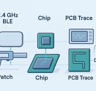
Patch vs Chip vs PCB Antenna for BLE Wearables (2026): What survives near the body?
2026-03-17
901
If your BLE wearable drops out the moment it hugs skin or slips under a sleeve, the antenna wasn’t chosen for the real world. This comparison focuses on what matters most for product leads and PMs: consistent range near the human body, detuning from plastics and nearby metal, certification risk, cost, and schedule predictability.
Key takeaways
l No single winner. The right choice depends on near
body use, enclosure and ground size, certification path, and budget.
l Chip antennas are compact and predictable when you honor keep
outs and ground rules; they often cut tuning iterations versus custom traces.
l PCB trace or inverted
F antennas minimize BoM but are highly sensitive to ground size and the enclosure; expect more tuning cycles.
l Patch and patch
like solutions can deliver higher directional gain and more stable on
body beam patterns when given enough ground/volume.
l Validate on body. Do fast VNA sweeps with a tissue phantom, then chamber TRP checks at 2402/2440/2480 MHz before freezing ID.
Quick verdict: when each antenna type wins near the body
Ultra
compact design with frequent enclosure tweaks: Favor a well
documented chip antenna. It’s small, keeps performance predictable if you respect edge placement and keep
outs, and usually needs only a modest matching network.
Disposable, lowest
cost beacon on plastic with decent board edge length: Choose a tuned PCB inverted
F. Unit cost is essentially free, but budget time for geometry edits and retunes as industrial design evolves.
Wrist
worn device where the phone is often body
obscured: Consider a patch or patch
like near
body solution. With adequate ground and height, you can improve realized gain and tame body
shadowing. Validate patterns on
wrist, not just on the bench.
Beacon near metal or inside tight plastic where detuning is unavoidable: A vetted chip antenna, including over
ground variants, tends to be the least risky—provided you follow the vendor’s layout notes and verify in
enclosure.
Fastest certification path using a pre
certified BLE module: Stick with the module’s listed antenna type and configuration. Changing type/gain/pattern can trigger additional testing in most regimes, lengthening timelines.
Side
by
side: patch vs chip vs PCB antenna for BLE
Below, equal
field comparison focused on what product teams ask most.
Dimension
Patch
Chip (SMD)
PCB Trace / Inverted
F
Near
body stability
With adequate ground/height, variants can keep on
body beams more stable; still validate
Predictable if keep
outs and ground length are respected; verify on
body
Highly sensitive to body/enclosure; biggest swings if layout shifts
Radiation coverage on body
More directional; variants can limit deep nulls
Quasi
omnidirectional at board edge; body can create nulls
Quasi
omnidirectional; enclosure and ground easily distort pattern
Efficiency and gain in free space
Can reach higher directional gain on suitable grounds
Typically modest peak gain on small boards
Good if you have space and careful tuning
Size and footprint
Taller; needs volume to shine
Smallest radiator; defined clearance window
Zero BoM; consumes long board edge and keep
out area
Ground and clearance sensitivity
Moderate; requires volume and spacing
High; violating keep
outs quickly hurts performance
High; geometry and ground size dominate results
Tuning effort and iteration risk
Moderate; usually stable once volume is set
Lower when rules are followed; 1–3 matching parts are typical
Higher; expect copper edits and more spins
Certification risk and time
Directional gain may affect exposure margins; plan pre
scans
Predictable with modules if unchanged vs reference
Changes frequently force re
evaluation; more surprises
Manufacturing repeatability
Good with consistent module construction
High (ceramic LTCC tolerances)
Depends on PCB process, finish, and soldermask
Unit cost (2026 snapshot)
Medium to higher vs chip in many cases
Low to medium
Lowest (board copper only)
Best for
Wrist
worn, body
shadowed use with room for volume
Compact wearables with evolving ID and schedule pressure
Cost
sensitive beacons with ample edge length
What really changes on body: detuning, patterns, and efficiency
Human tissue is lossy at 2.4 GHz. Place any antenna within a few millimeters of skin and you’ll shift resonance, narrow bandwidth, and sap efficiency. Vendor guides warn plainly that nearby dielectric and conductors detune antennas and that metallized plastics and tight clearances are risky; see the practical cautions in NXP’s compact planar hardware notes in the official application guidance and user guides. For example, "do not route ground or traces beneath the radiator" and "test plastics early for RF loss" are recurring themes in the guidance provided by the NXP engineering notes and user materials you’ll find in their antenna design literature.
On pattern stability, academic work on wearable patch variants shows how engineered surfaces can stabilize on
body beams. In a comparative wearable study, patch designs using surface features reported materially different on
body main
lobe behavior compared with conventional patches, underscoring that structure and spacing matter on skin, not just in free space. See the on
body pattern results discussed in the peer
reviewed analysis of wearable dual
band patch antennas available via the National Library of Medicine.
If you’re wrestling with detuning, matching still matters. A solid primer on 50
ohm PCB antenna matching and practical optimization can help teams set up a fast pre
scan workflow before booking chamber time. For a walkthrough of theory to hands
on tuning steps, see the internal guide titled "How can we achieve 50
ohm impedance matching in PCB antenna design— from theory to practical optimization," published by the Kinghelm team.
Antenna type deep dives
Chip antennas
Chip antennas shine in tight spaces when you follow the playbook: edge placement, a clean keep
out window, and a grounded coplanar 50
ohm feed with via fencing. Authoritative vendor primers explain why the ground plane forms part of the radiator and why even small clearance violations crush efficiency; they also show that a modest 1–3 component matching network is usually enough when the rules are respected. For a concise technical overview of how chip antennas work, common pitfalls, and integration patterns, consult the Understanding Chip Antennas handbook provided by Johanson Technology.
For buyers and PMs, here’s the deal: chip antennas reduce iteration risk when your industrial design is still changing. You can often carry a vetted footprint across SKUs with predictable updates to the matching network—so long as you preserve the ground geometry and keep
outs.
Consideration for near
body use: despite predictability, body loading can still shift resonance and create nulls. Plan a quick on
wrist VNA sweep and a three
point TRP sample before committing.
Relevant resource: Explore example form factors and layout references in the Kinghelm SMT antenna category to see the range of edge
mount geometries teams commonly adopt.
PCB trace and inverted
F
A printed inverted
F gives you the lowest unit cost. But you "pay" in schedule and layout sensitivity. Geometry, edge length, and nearby plastic or metal can swing performance widely. Practical design guides from MCU and RF vendors detail the coplanar 50
ohm feed, no
ground zones, and meander/length trade
offs needed to hit resonance, along with the warning that small enclosure changes can force copper edits. If you’ve got 20–30 mm of clean board edge and stable plastics, traces can perform well—and they’re nearly free on the BoM.
Caveat for wearables: proximity to skin and small grounds push IFAs into a tight corner. Expect more tuning cycles and larger free
space
to
on
body deltas than with a well
integrated chip solution.
Patch antennas
Patches earn their keep when you can afford some height and ground area. Directional realized gain and beamwidth can help punch through body shadowing, especially in wrist
worn or torso
adjacent use. Peer
reviewed wearable studies comparing conventional and engineered patch variants have demonstrated more stable on
body beams, backing the intuition many RF teams already have from the chamber.
Compact SMD patches exist; on very small grounds their peak gain can be modest, but the pattern benefits may still help in difficult orientations. Many product teams trial a compact patch alongside a chip to see which integration wins on net once the enclosure is final.
Resource for scoping options: Review options in the Kinghelm Bluetooth patch antenna category to understand the envelope and mechanical trade
offs typical for small wearables.
Certification and SAR: how antenna choice affects risk
For EU markets, 2.4 GHz radios must meet the essential transmitter and unwanted emissions requirements defined in EN 300 328. Your antenna changes EIRP, bandwidth usage, and OTA emissions profiles—so expect those to be verified over the air. When using pre
certified modules, keeping the same antenna type and gain pattern that the module lists generally simplifies your path; deviating can trigger additional testing.
Wearables near the body may also require SAR assessment depending on transmit power, duty cycle, and separation distance. Placement that concentrates fields near tissue pushes you toward pre
scans earlier in the program. A practical approach: book a short lab session once your enclosure and antenna placement are roughly set, and treat that as a go/no
go gate for ID freeze.
Practical testing plan that fits real schedules
Start with a fast benchtop loop: tune to 50 ohms on the VNA in free space, then repeat with a tissue phantom 0–5 mm from the enclosure to estimate resonance shift and bandwidth changes. Next, grab chamber time for a three
frequency TRP sample at 2402, 2440, and 2480 MHz, comparing free space to on
wrist or on
phantom configurations. Finally, run a simple range walk in a cluttered office with the device worn as intended, logging RSSI while you vary orientation. This sequence gives PMs a clear picture of detuning risk and orientation sensitivity without stalling industrial design.
FAQ
l Which antenna is best for wrist
worn BLE devices near skin? If you have the volume, a patch or patch
like solution can improve realized gain and stabilize on
body beams, but always validate patterns and SAR early. When volume is tight, a well
integrated chip antenna is the pragmatic choice.
l How much does the human body detune a 2.4 GHz antenna? It depends on spacing and materials; expect measurable resonance shifts within a few millimeters of skin and meaningful efficiency loss. That’s why tissue
phantom pre
scans and on
body TRP checks are table stakes before design freeze.
l Can I keep certification if I swap the antenna on a pre
certified BLE module? If you retain the listed antenna type and comparable gain/pattern, re
use is often possible; changing type, gain, or placement typically triggers additional evaluation. Plan time for a lab consult when considering changes.
l I cracked an SMD BLE antenna during rework. What now? For a practical field repair and replacement walkthrough, see this neutral troubleshooting guide on common SMD antenna breakage and how teams typically address it from the Kinghelm knowledge base.
Sources and further reading
l Chip antenna integration principles and pitfalls are well summarized in the Understanding Chip Antennas technical handbook by Johanson Technology.
l Practical IFA layout and enclosure cautions are covered in NXP’s official user guides and application notes for compact planar antennas.
l Wearable patch behavior on body is documented in a peer
reviewed comparative analysis of dual
band patch antennas hosted by the National Library of Medicine.
l EU transmitter performance and OTA verification requirements are defined in EN 300 328.
Also consider vendor resources and reference layouts when shortlisting parts. Reviewing a chip footprint library or a compact patch option early can shorten your spin count and smooth certification. When in doubt, validate on body, then decide.
Understanding Chip Antennas — Johanson Technology
NXP BLE antenna design user guide
Taoglas application note on enclosure proximity and clearances
Wearable dual
band patch antenna comparative study (MDPI/PMC)
ETSI EN 300 328 v2.2.2 specification
Explore chip antenna form factors: Kinghelm SMT Antenna category
Patch options and envelopes: Kinghelm Bluetooth Patch Antenna category
Matching and pre
scan primer: 50
ohm PCB antenna matching — theory to practice
SMD antenna field repair: What to do if your Bluetooth SMD antenna breaks
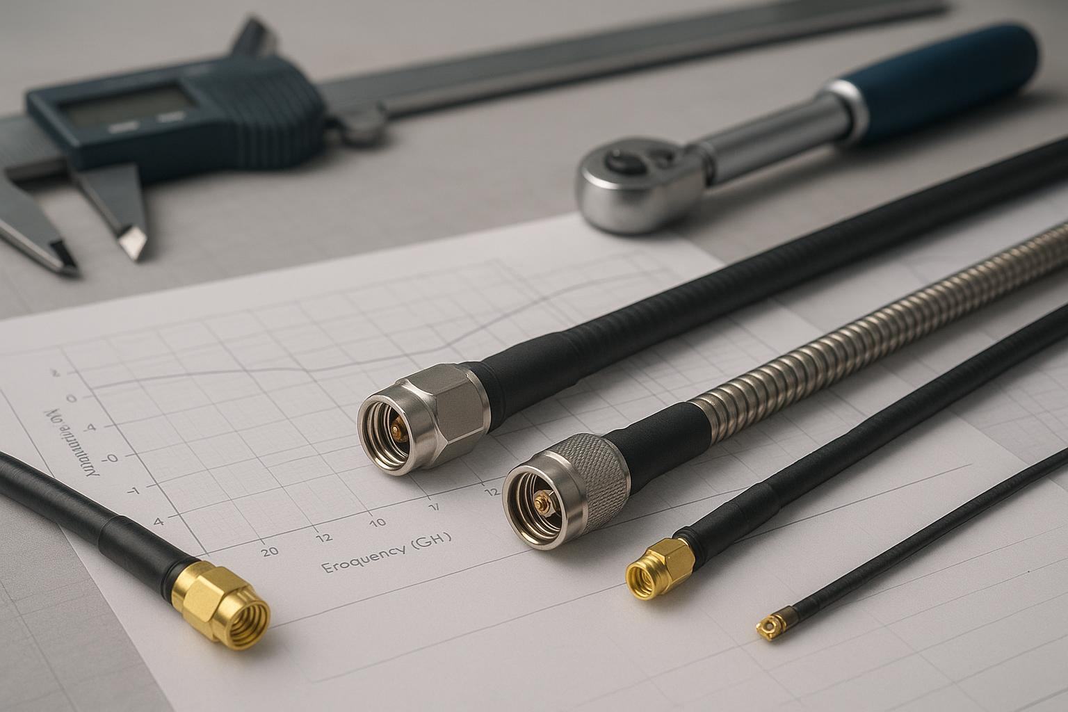
RF Coaxial Cables Explained: Types, Uses, and Maintenance
2026-03-10
848
If you’re buying for RF systems, RF coaxial cables quietly determine link budget, uptime, and total cost of ownership. The right line size and connectorization keep VSWR low, trim losses at your highest operating frequency, and stand up to the environment your project lives in. This guide translates engineering requirements into purchasing criteria you can use in RFQs and vendor reviews—so your RF coaxial cables deliver predictable performance throughout their lifecycle.
Key takeaways
●Start with frequency and run length, then size attenuation; verify power handling, impedance, connector interfaces, and environment before you issue an RFQ.
●Use datasheet attenuation at your top frequency to pick between families (e.g., LMR vs RG) and diameters; don’t rely on single-point "typical" figures.
●Maintenance discipline (cleaning, torque, bend radius, sealing) prevents avoidable VSWR spikes and downtime; set inspection and test expectations in contracts.
The quick primer on RF coaxial cables
Most buying decisions cluster around four families. Think of them as lanes on a highway: flexible RG for general traffic, low‑loss LMR for longer, faster lanes, semi‑rigid/formable for precision exits inside equipment, and corrugated hardline for the heavy trucks of infrastructure.
RG flexible lines are the classic general‑purpose series spanning 50 Ω (e.g., RG‑58, RG‑213) and 75 Ω (e.g., RG‑6, RG‑59) used in test leads, radio, and video. Loss varies widely by type and maker, so always compare like‑for‑like datasheets.
LMR low‑loss flexible cables are modern, well‑documented lines with accessories across sizes like LMR‑240 and LMR‑400. Times Microwave’s family guides outline construction and performance across variants such as FR, UF, and DB for different environments, with consistent attenuation tables by frequency in the datasheets. See the manufacturer’s overview in the LMR complete guide (Times Microwave, 2024).
Semi‑rigid and formable cables deliver precise, stable phase for internal interconnects; they offer excellent repeatability but limited flexibility.
Corrugated hardline serves infrastructure feeders for very long runs and high power; it offers extremely low loss but larger bend radii and specialized connectors.
Two system traits steer early choices for RF coaxial cables:
●50 Ω vs 75 Ω: Most radio and data links are 50 Ω; broadcast/video and CATV are 75 Ω. Mixing them raises reflections unless you add matching pads or adapters. For an approachable overview of use cases, see Fairview Microwave’s basics of BNC connectors.
●Connector landscape: Expect SMA and N for 50 Ω RF; TNC in ruggedized runs; BNC for lab/video; MCX/MMCX in compact gear; miniature IPEX/U.FL on modules.
Mini comparison at 1 GHz (typical values per datasheet):
Cable
Attenuation at 1 GHz (dB/100 ft)
Primary source
LMR‑240
9.9
Times Microwave LMR‑240 datasheet
LMR‑400
5.1
Times Microwave LMR‑400 datasheet
Those figures help you sanity‑check run lengths: for the same frequency and length, the larger‑diameter LMR‑400 loses roughly half the power that LMR‑240 does.
A procurement selection framework for RF coaxial cables
Here’s a simple way to reach a defensible choice without getting lost in equations.
1.Frequency and run length → attenuation budget
●Identify your highest operating frequency and the maximum acceptable path loss across the cable. Use datasheet attenuation at that frequency, scaled to your planned length, to shortlist families and diameters. If you’re on the fence between two sizes, check the next frequency octave, too.
2.Power handling and dielectric
●Confirm continuous‑wave and peak power ratings at your frequency. Higher frequency raises dielectric loss and heating; keep a margin if ambient temperatures are high or runs are bundled.
3.Impedance match and adapters
●Keep the system consistent (50 Ω or 75 Ω) end‑to‑end. If you must mix, insert proper matching pads; otherwise, expect degraded return loss.
4.Shielding, PIM expectations, and test method
●Specify shielding construction (foil plus braid for wideband shielding) and, if you’re in cellular or other sensitive services, ask for passive intermodulation test results using the IEC 62037 method family. The standard defines the two‑tone measurement approach; acceptance levels are set by your application and vendor spec. See IEC 62037 series overview (IEC Webstore) for scope and method references.
5.Environment, jacket, and compliance
●Outdoor runs benefit from UV‑resistant PE jackets; indoor plenum/vertical shafts may dictate FR or LSZH variants. Call out temperature range, UV, and safety listings (UL/CSA/CPR) in the RFQ.
6.Connectors and assembly quality
●Name the interfaces (e.g., SMA to N) and materials. Assembly workmanship matters: proper crimp/solder, strain relief, and torque. As a reference point, Amphenol RF lists SMA plug mating torque ranges depending on materials; verify the exact value on your connector’s datasheet. See Amphenol RF on SMA connectors for guidance.
7.Vendor documentation
●Require current datasheets with attenuation tables, bend radii (installation vs repeated), power handling, temperature range, test results (VSWR and PIM if relevant), and compliance statements (RoHS/REACH and safety listings).
Suggested RFQ boilerplate you can adapt:
Cable assembly requirements- System: 50 Ω (or 75 Ω), operate to [max frequency] GHz.- Run length: [L] m/ft; max total cable loss ≤ [X] dB at [max frequency] GHz.- Cable family/size: [preferred family/size], alternatives allowed if loss and bend radius meet targets.- Connectors: [interface/material/plating] at source → [interface/material/plating] at load; include recommended mating torque in datasheet.- Environment: [indoor/outdoor], jacket [PE/FR/LSZH], operating temp [min..max] °C, UV rating [if outdoor].- Tests: Provide VSWR sweep to [max frequency] GHz; if applicable, PIM per IEC 62037 with stated conditions and acceptance level.- Documentation: Attenuation table; min bend radius (install/repeated); power handling at [freq]; compliance (RoHS/REACH, UL/CSA/CPR as applicable).
The specs that matter and how to read them
Attenuation and sizing
●Use the manufacturer’s attenuation at your top frequency, scaled to length, to choose a diameter. For example, per Times Microwave datasheets, LMR‑240 is 9.9 dB/100 ft at 1 GHz and LMR‑400 is 5.1 dB/100 ft at 1 GHz. That difference can make or break a tight link budget. Check the actual PDFs: LMR‑240 datasheet and LMR‑400 datasheet.
Power handling and heat
●Power ratings fall with frequency as dielectric loss rises. Stay conservative if you expect high ambient temperatures or bundling. When in doubt, ask the vendor for derating curves or a worst‑case figure at your frequency.
Impedance and return loss
●Keep 50 Ω or 75 Ω consistently across cable and connectors. If you must join worlds, a matching pad prevents hard reflections. For a clear, vendor‑neutral explainer of where each impedance is common, see Fairview Microwave’s BNC connector basics.
Shielding effectiveness and PIM
●Foil‑plus‑braid constructions improve wideband shielding and help keep coupled noise down. In cellular and other sensitive systems, specify low‑PIM assemblies and request test data using the IEC 62037 methodology; acceptable levels vary by application and must be stated in the RFQ and vendor response.
Bend radius
●Datasheets often distinguish "installation" versus "repeated" bend radius. For instance, Times Microwave lists LMR‑240 at 0.75 in (install) and 2.5 in (repeated), and LMR‑400 at 1.0 in (install) and 4.0 in (repeated). Those values come directly from the manufacturer PDFs cited above; route accordingly and call these limits out in drawings.
Connectors and torque
●Under‑ or over‑torqueing is a common cause of intermittent VSWR. As a benchmark, SMA interfaces typically specify mating torque within narrow ranges that depend on materials; confirm on the connector datasheet. Amphenol RF’s SMA page provides representative ranges and handling guidance.
Maintenance SOPs to keep VSWR low
You’ll save money and outages by setting handling expectations in purchase orders and maintenance contracts. Here’s a practical baseline you can tailor with your vendors and O&M partners.
Cleaning and contact care Keep mating planes and threads clean; remove metallic particles after any cable cutting before connectorization. Keysight explains good hygiene for cable and antenna measurements in an application note; see Keysight’s measurement hygiene guidance. Cleanliness is one of the fastest ways to keep RF coaxial cables performing to spec.
Torque and strain relief Use preset torque wrenches for threaded connectors; add strain relief to avoid torsion at the back shell. A concise field‑focused read on common pitfalls is Kinghelm’s 7 common SMA connector mistakes.
Bend radius and routing Respect both installation and repeated‑bend minima (the LMR‑240/400 figures above illustrate why). Avoid tight service loops that creep below the repeated radius. Over‑bending RF coaxial cables invites micro‑kinks and impedance discontinuities that show up as VSWR spikes later.
Weatherproofing and sealing Outdoor joints need boots or tape kits and UV‑resistant jackets; re‑inspect after seasonal extremes. Call for resealing after connector maintenance.
Inspection and test cadence As a policy default, do quarterly visual checks on outdoor runs and an annual sweep test to the system’s top frequency. Treat this as a starting point and adjust based on environment and vendor O&M guidance.
Practical scenarios and one neutral example
Scenario 1 — Indoor Wi‑Fi module to panel antenna
●Requirement: 2.4/5 GHz, 1.5 m run inside an enclosure with occasional servicing. Loss target ≤1.5 dB at 5 GHz. Interfaces: IPEX/U.FL at the module, SMA bulkhead at the panel.
●selection: Favor a 50 Ω low‑loss flexible line such as an LMR‑200/240‑class jumper over micro‑coax if routing space allows; specify FR jacket if the enclosure demands it. Call out SMA mating torque and the repeated bend radius for the chosen cable in the RFQ. Vendors such as Kinghelm offer IPEX↔SMA jumpers and related connectors you can evaluate against these criteria.
Scenario 2 — Rooftop cellular repeater feed
●Requirement: Several tens of meters outdoors; high duty cycle near band tops. Loss and PIM sensitivity dominate.
●selection: Step up in diameter (e.g., LMR‑400‑class or corrugated hardline) to control attenuation; require UV‑resistant jackets, low‑PIM test data per IEC 62037, and weatherproofed connectors.
Scenario 3 — Indoor DAS jumper
●Requirement: Short, flexible jumpers with repeatable performance.
●selection: Prefer flexible low‑loss jumpers with documented repeated bend radii; specify connector torque ranges and periodic replacement after a defined cycle count.
Next steps
●Convert system limits into procurement criteria: top frequency, acceptable cable loss, environment, connector interfaces, and any PIM expectations.
●Use the RFQ snippet above and insist on datasheets with attenuation tables, bend radii, and torque guidance.
●If you need a starting point for off‑the‑shelf assemblies and connectors to benchmark, browse Kinghelm’s products overview and compare options using the checklist you’ve built. Along the way, keep repeating the simple rule: size RF coaxial cables by frequency and length first, then confirm the rest.
Pogo pin charging dock reliability guide for test engineers
2026-03-03
939
Daily charge cycles, sweat, pocket lint, and casual abuse make wearable charging docks one of the harshest "small" interfaces in consumer electronics. If your goal is 100k to 1M reliable mates, you need more than a spec sheet—you need repeatable tests, tight acceptance criteria, and maintenance habits that hold up on the line and in the field. This guide, written from a manufacturing and reliability perspective, shows how to qualify and sustain pogo-pin docks for long life without guesswork.
Key takeaways
l Target and measure what matters: four-wire contact resistance, drift over life, spring force retention, working stroke margin, and temperature rise under load.
l Anchor your plan to recognized methods: durability, contact resistance, and current-carrying capacity from the IEC 60512 series, plus salt mist per IEC 60068-2-11 for sweat-like corrosion.
l For sweat-exposed wearables, prefer gold-over-nickel plating with functional thickness around 50–100 µin as a starting point, validated by salt fog and biased cycling.
l Practical starting criteria: initial contact resistance ≤20–30 mΩ, ΔR ≤20 mΩ after 100k cycles, nominal force per pin ~0.8–2.0 N with ≥80% retention at 100k, and ≤20–30 °C rise at rated current after 30 minutes steady-state.
l Production success depends on process: incoming AQL checks, in-line SPC on resistance and alignment, and a simple cleaning SOP keep fixtures and docks on-spec.
What reliable means for wearable docks
Reliability is not an abstract promise; it is a set of measurable limits you can verify at the bench and monitor in production. Here is a concise acceptance matrix to tune for your product and supplier. Treat these as starting values to be confirmed against your chosen pogo part numbers and real data.
Metric
Target at start of life
Target over life
Contact resistance (4-wire, 100 mA)
≤20–30 mΩ preferred; ≤50 mΩ acceptable for very small pins
ΔR ≤20 mΩ after 100k; aim to keep absolute R <100 mΩ through intended life
Spring force at working height
0.8–2.0 N per pin typical for wearables
≥80% retention after 100k cycles
Working stroke
0.5–1.0 mm recommended
≥0.3 mm headroom to avoid bottoming at full compress
Temperature rise at rated current
Define per design current
≤20–30 °C after 30 minutes steady-state
Environmental corrosion and wear
Visual: no red rust on functional surfaces
Post-exposure resistance within limits
These values align with widely used connector tests in the IEC 60512 series for durability, contact resistance, and current-carrying verification, and environmental exposures such as salt mist in IEC 60068-2-11.
Design choices that pay off across 100k to 1M cycles
Think of long life as a budget: every mating cycle spends a bit of plating, spring preload, and alignment tolerance. Good design spends wisely.
l Geometry and alignment: Use guiding chamfers or a shallow pocket with magnet assist to land pins within their sweet-spot stroke. Set the nominal working stroke around the mid-travel, not near bottoming.
l Spring force: For compact wearables, 0.8–2.0 N per pin balances consistent contact resistance with manageable user force. Confirm force at the working height, not only at full travel, and specify retention after cycling.
l Plating system: Default to gold over nickel for low resistance and corrosion protection. For high-cycle docks, functional gold thickness in the 50–100 µin range (with a robust nickel underlayer) is a practical starting point; validate thickness and hardness with your supplier and tests.
l Current path and heat: If you need higher charge currents, distribute load across multiple pins in parallel and verify temperature rise under continuous current. Keep the mechanical stack rigid enough to maintain uniform compression under load.
l Sealing and contaminants: If the wearable or dock claims water resistance, prioritize gasket design, drainage paths, and keepout zones that prevent standing moisture around the contacts.
Lab protocol for pogo-pin lifecycle testing
Use a protocol you can reproduce in any lab and explain in an audit. The goal is to correlate changes in contact resistance and force with visible wear and environmental stress.
1. Build or commission a cycling fixture that controls alignment and stroke. Set nominal working stroke (for example 0.7 mm) at the dock’s mechanical center, with 250–500 ms dwell at compression and 10–20 cycles per minute.
2. Instrument the DUT with four-wire Kelvin measurement at a defined current, such as 100 mA. Log resistance at a fixed compression point every 1k–5k cycles, and capture min/mean/max.
3. Add a periodic spring-force check using a calibrated force gauge at the working height. Record force retention trends.
4. Inspect under magnification for debris, plating wear, and bent or sticking pins at defined intervals. Clean only per your maintenance SOP to avoid masking early failures.
5. At milestone counts—say 100k, 250k, 500k, and 1M—run a steady-state current test and log temperature rise at the hottest point.
When you document, state the standard method names you’re aligning to for durability and resistance. Referencing the IEC 60512 series for durability and contact resistance clarifies expectations for reviewers and suppliers.
Environmental conditioning and combined stress
Pogo pins in wearables face sweat chemistries, humidity, temperature cycling, and occasional shock or vibration. Combine these exposures with cycling to avoid optimistic bench-only results.
l Salt mist corrosion: Run a controlled salt fog exposure, then rinse, dry, and re-measure. IEC 60068-2-11 Test Ka specifies a 5% NaCl solution in a 35 °C chamber with controlled pH; select 48–96 hours based on severity and material choices.
l Damp heat steady state: Use 85 °C and 85% RH to stress porosity and diffusion pathways in plating stacks. Measure before, during if feasible, and after exposure.
l Thermal shock: Alternate low and high temperatures appropriate to your product to induce differential expansion and potential micro-cracking in platings or solder joints.
l Vibration and mechanical shock: Validate the assembled dock at the device level to ensure blind-mating repeatability and contact stability under motion.
l Current loading under environment: After each environmental step, repeat a 30-minute current test and confirm the temperature rise remains within limits.
Production QA that sustains reliability targets
Reliability in the field starts with disciplined verification at incoming and continues with light-touch controls on the line.
l Incoming inspection: Use AQL sampling tuned to risk for electrical, force, and key dimensions. For critical electrical checks, consider tightened levels and very low AQL values; for visuals, a higher AQL may be acceptable. Record lot traceability and all measurement conditions.
l In-line checks and SPC: Spot-check contact resistance and alignment at defined intervals, and chart the data. Escalate inspection frequency or hold shipments if you see trend drift.
l Documentation and fixtures: Keep force-measurement jigs and 4-wire probes calibrated. Where lots are very small, consider 100% verification rather than statistical sampling.
Maintenance and field service to extend life
A simple, consistent cleaning SOP often adds more life than exotic platings. Use non-abrasive tools and solvents that do not damage gold.
l Tools and solvents: Prefer dry air, anti-static brushes, and lint-free swabs. For grime, use isopropyl alcohol sparingly, or soap and DI water where allowed, and then dry thoroughly.
l What to avoid: Harsh, acidic, or abrasive cleaners that thin or scratch plating. If a supplier warns against specific solvents on gold contacts, follow their guidance.
l Replace vs refurbish: If resistance remains high after cleaning, if pins stick or fail to rebound, or if force drops below your acceptance limit, replace the contact set or dock insert.
Troubleshooting high resistance and intermittent charge
Here’s the deal: rising resistance usually traces back to one of four culprits—contamination, wear-through of plating, loss of spring force, or misalignment. Start with a controlled clean and re-test at the working stroke. If resistance recovers temporarily and then drifts, suspect plating wear and validate thickness or hardness. If force is low at height, measure and log spring set; replace contacts and review force spec. If resistance varies with slight side load, investigate alignment, magnet bias, and housing tolerances.
Case note a 200k-cycle validation snapshot
In one bench program, a five-pin dock cycled at 15 cycles per minute to 200k mates with 0.7 mm working stroke. Initial mean contact resistance was 22 mΩ per pin. After 200k cycles, mean increased to 36 mΩ with a standard deviation of 5 mΩ; no pin exceeded 60 mΩ. Spring force at working height dropped from 1.4 N to 1.2 N, within an 85% retention target. A 1.5 A steady-state current test produced a 14 °C rise at the hottest point. Post-test inspection showed light polishing marks with no visible base-metal breakthrough. The take: acceptance targets were met, but the upward trend indicates you should re-verify at higher counts and after salt fog to confirm margin.
Vendor data points to calibrate expectations
l Temperature rise and contact resistance: A discrete spring-loaded pin example lists 9 A at a 30 °C temperature rise limit and 20 mΩ typical initial contact resistance; use this to bound your own ΔT and voltage-drop limits in higher-current cradles.
l Plating thickness guidance: Connector plating specialists note that 50–100 µin functional gold thickness over a robust nickel underlayer is common for high-duty contacts intended to resist wear and corrosion; confirm actual thickness on your selected part.
l Pogo pin catalogs often position "high mating cycles," but device-size details vary; always pull the exact datasheet for stroke, force at height, and any published endurance notes.
Accordingly, build your plan around standards-based methods and verify the specifics with supplier datasheets and your own test runs.
Define pogo pin charging dock reliability in one plan
To lock down pogo pin charging dock reliability, write a short validation plan that names the tests, limits, and sample sizes in one place. Include the durability and resistance methods from the IEC 60512 series, salt mist per IEC 60068-2-11 for corrosion, steady-state current-carrying verification with a ΔT limit, and explicit acceptance numbers for resistance drift and force retention. Then mirror those limits in your incoming and in-line QA instructions so production stays aligned with qualification.
Tooling and supplier checklist
Ask every candidate supplier for the same set of facts so you can compare apples to apples: plating system and verified gold thickness, nickel underlayer thickness, initial contact resistance and its measurement method, force at the intended working height with tolerances, total and working stroke, any published endurance numbers with the test method used, and the recommended cleaning solvents. For your lab, maintain a cycling fixture with stroke control and counters, a calibrated force gauge accessory, four-wire probes with stable fixturing, a temperature probe or IR camera for ΔT checks, and a simple data-logging script that timestamps every sample.
Related reading
If you are mapping adjacent connector families used alongside pogo interfaces, these overviews from My Brand provide neutral context:
For micro RF coax jumpers sometimes present near charging ports, see the explainer on IPEX sizes and use cases in Understanding IPEX 1 and IPEX 4 Connectors on the My Brand site: Understanding IPEX 1 and IPEX 4 Connectors.
For context on miniature RF connectors paired with low-profile docks, review this comparison article benchmarking MCX and MMCX styles: Amphenol benchmark against Kinghelm MCX and MMCX connector.
Sources and standards for deeper reference
For durability and contact-resistance test naming and scope, see the IEC 60512 series overview in the EN 60512-1-100 catalog page published by IEC in 2012: IEC 60512 series overview.
For a concrete current and ΔT example and typical contact-R, consult the Mill-Max 0965 discrete spring-loaded pin datasheet: Mill-Max 0965 datasheet.
For plating thickness guidance across connector duty cycles, see Advanced Plating Tech’s education page on gold thickness for connectors: Gold plating thickness for connectors.
For salt fog parameters used in corrosion screening, IEC 60068-2-11 Test Ka outlines the 5% NaCl, 35 °C chamber conditions: IEC 60068-2-11 Test Ka parameters.
For practical cleaning and handling guidance on spring-loaded contacts, Mill-Max summarizes do’s and don’ts in their FAQ: Spring-loaded pogo pin FAQs and cleaning.
For an overview of AQL concepts and how they pair with SPC in electronics, see this practitioner guide: Acceptable Quality Limit fundamentals.
Next steps
Draft a one-page validation and QA plan this week, order sample lots from two pogo suppliers, and schedule your first 100k-cycle run. If you need broader connector context for your team, My Brand maintains educational overviews on adjacent connector types at kinghelm.net.
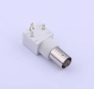
BNC Connectors: A Procurement Guide for Reliable RF and Video Interconnect Solutions
2026-02-24
887
In modern electronic systems, reliable signal transmission is fundamental to performance, safety, and product longevity. Among the many interconnect solutions available, the BNC (Bayonet Neill–Concelman) connector remains one of the most widely used coaxial connectors across test equipment, telecommunications, video systems, and industrial electronics. For procurement professionals responsible for sourcing electronic components, understanding the characteristics, selection criteria, and supplier landscape of BNC connectors is essential to ensuring stable production and long-term system reliability.
Overview of BNC Connector Technology
The BNC connector is a miniature quick-connect RF connector featuring a bayonet coupling mechanism. Unlike threaded connectors, the BNC design allows a secure connection through a simple push-and-twist action, enabling fast installation while maintaining resistance to vibration and accidental disconnection. This combination of convenience and reliability has made it a standard interface for coaxial connections for decades.
BNC connectors are typically manufactured in two impedance variants: 50 ohms and 75 ohms. The 50-ohm version is commonly used in RF, wireless communication, and test instrumentation, where power handling and signal integrity are critical. The 75-ohm version is primarily used in video transmission applications such as broadcast equipment and CCTV systems, where impedance matching minimizes signal reflections and ensures image quality.
Typical Application Scenarios
BNC connectors are present in a wide range of professional and industrial environments. In test and measurement equipment, they serve as standard interfaces for oscilloscopes, signal generators, and spectrum analyzers. In video and surveillance systems, they remain a dependable choice for analog cameras and transmission equipment due to their secure locking mechanism and stable impedance characteristics. Telecommunications infrastructure and RF systems also employ BNC connectors for antenna connections, radio equipment, and signal distribution.
Industrial automation and medical electronics frequently utilize BNC connectors for monitoring systems, control interfaces, and diagnostic devices, where durability and consistent performance are required over extended operating periods. Because these applications often involve mission-critical equipment, procurement decisions must emphasize reliability and lifecycle stability rather than simply unit price.
Key Factors in BNC Connector selection
selecting the appropriate BNC connector involves evaluating both electrical performance and mechanical compatibility with the intended system design.
Impedance matching is the first and most critical parameter. Using a connector with incorrect impedance can introduce signal reflections, attenuation, and performance degradation. Procurement teams should always confirm system requirements with engineering documentation before placing orders.
Mounting configuration is another important consideration. Cable-mount connectors are typically used for field-terminated cables and patch leads, panel-mount or bulkhead connectors are designed for equipment enclosures, and PCB-mount versions allow direct integration onto printed circuit boards. Standardizing mounting styles across product lines can simplify inventory management and reduce assembly complexity.
Termination method also affects manufacturing efficiency and long-term reliability. Crimp termination is commonly preferred in high-volume production environments due to its consistency and speed, while solder termination may be selected for specialized applications requiring maximum electrical integrity.
Material selection influences both durability and environmental performance. Connectors with nickel or gold plating provide corrosion resistance, while brass or stainless steel bodies offer mechanical strength. High-quality dielectric materials ensure stable impedance and insulation characteristics across temperature ranges.
Frequency capability should also be evaluated, particularly for RF applications. Standard BNC connectors typically operate effectively up to approximately 4 GHz, although precision variants may support higher frequencies.
Supply Chain and Quality Considerations
From a procurement perspective, connectors are often high-volume components with long lifecycle requirements. Therefore, supplier reliability is as important as product specifications. Stable production capacity, consistent quality control, compliance with international environmental regulations such as RoHS and REACH, and predictable lead times all contribute to reducing supply risk.
It is also advisable to qualify multiple suppliers for critical components, ensuring continuity in case of disruptions. Packaging methods suitable for automated assembly and clear traceability documentation can further improve manufacturing efficiency and quality assurance.
Mainstream Brands in the BNC Connector Market
The global market for BNC connectors includes several well-established manufacturers known for performance and reliability. International brands such as Amphenol, TE Connectivity, and Molex are widely specified in high-end industrial and telecommunications equipment due to their extensive product portfolios and rigorous quality standards.
At the same time, cost-effective manufacturers have gained increasing recognition for offering competitive alternatives with reliable performance. Kinghelm, for example, provides a range of RF connectors including BNC types designed for applications in communications equipment, industrial electronics, and consumer devices. With an emphasis on quality consistency, durability, and compliance with international standards, such suppliers are often considered by procurement teams seeking to balance performance requirements with cost control.
Conclusion
Although BNC connectors are mature components, their role in ensuring stable signal transmission remains critical across numerous industries. Careful evaluation of impedance, mounting style, materials, frequency performance, and supplier reliability can significantly reduce the risk of system failure and production delays.
For procurement professionals, the optimal sourcing strategy combines technical suitability with dependable supply, long-term availability, and competitive pricing. By partnering with reputable manufacturers and maintaining clear specifications, organizations can ensure that even small components like connectors contribute positively to overall product quality and operational efficiency.
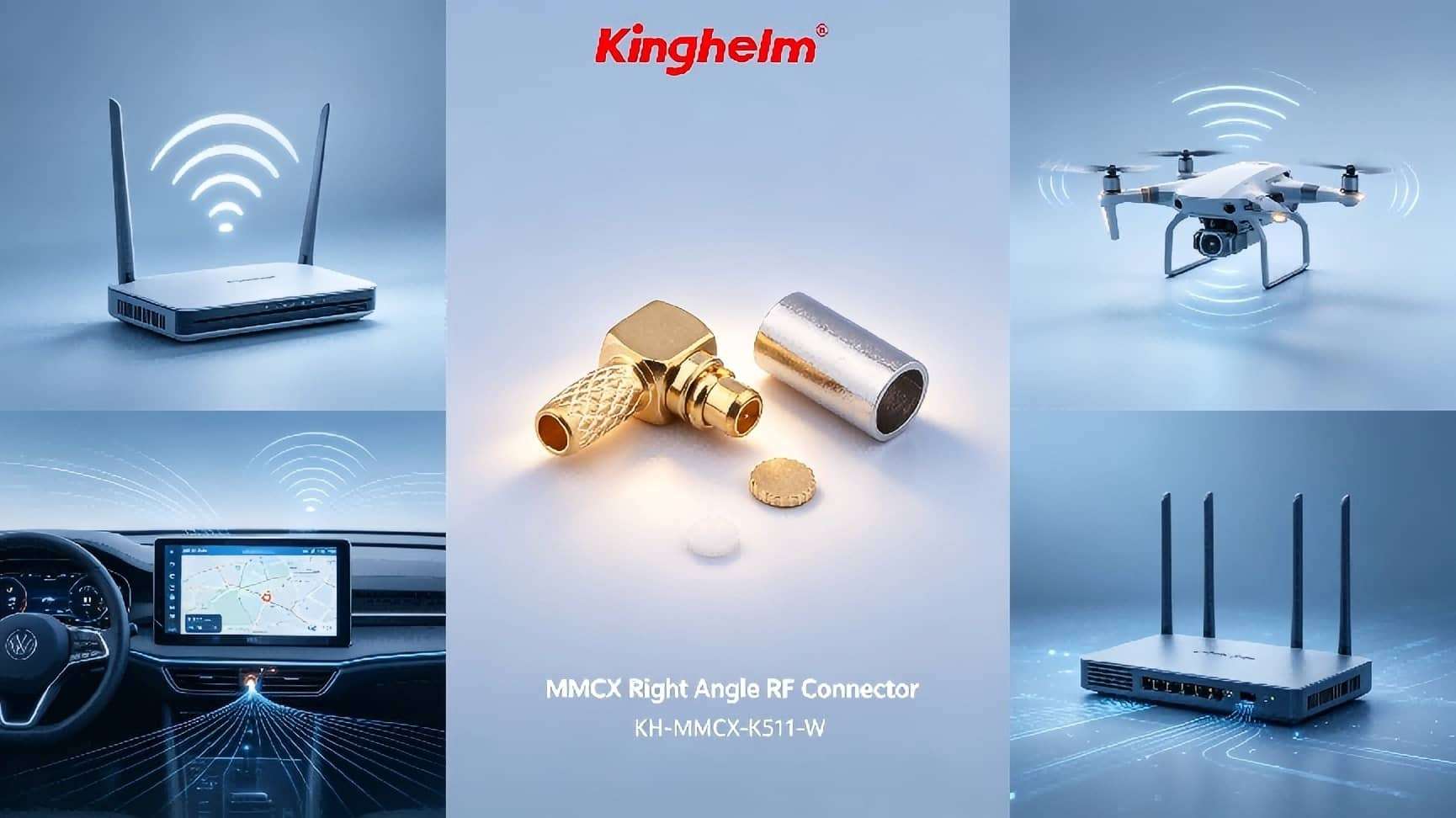
RF Connectors Explained: Types, Principles, and How to Choose the Right Coaxial Connector for RF & Microwave Applications
2026-04-23
919
KH-MMCX-K511-W
RF connectors (also called coaxial connectors or RF Connectors) are precision components engineered to carry radio-frequency signals while preserving shielding and minimizing signal reflection or loss. They form the critical interface between coaxial cables, antennas, test equipment, and RF/microwave circuits, ensuring consistent performance from DC up to tens of gigahertz.
For intermediate engineers, technicians, or system integrators working in telecommunications, wireless infrastructure, test & measurement, or microwave systems, understanding RF Connectors helps you select components that match your frequency, power, and environmental requirements—avoiding costly signal degradation or equipment damage.
What Are RF Connectors?
An RF Connector is an electrical connector designed for radio frequencies in the multi-megahertz range. It maintains the coaxial structure of the cable to prevent electromagnetic interference and keep impedance consistent.
How RF Connectors Work: Core Principles
RF Connectors operate by extending the transmission line without mismatch. Key performance factors include:
• Impedance matching — Prevents reflections.
• Shielding effectiveness — Blocks external noise.
• Mating mechanism — Threaded, bayonet, or snap-on.
• Frequency rating — Determines performance limits.
• Power handling & durability — Affects lifespan.
Properly mated connectors behave as a seamless extension of the coaxial line.
Common Types of RF Connectors
• BNC Connector: Quick-connect, up to 4 GHz.
• N-type Connector: Weatherproof, up to 11–18 GHz.
• SMA Connector: Compact, up to 18–26.5 GHz.
• MCX / MMCX: Small snap-on connectors.
• IPEX (u.FL): Ultra-mini PCB connectors.
• FAKRA: Automotive RF applications.
How to Choose the Right RF Connector
• Frequency and VSWR requirements
• Impedance (50Ω / 75Ω)
• Environment and durability
• Size and connection type
Always verify datasheets before final selection.

Kinghelm DIP Switches for Consumer Electronics | Reliable & Cost-Effective Configuration
2026-02-03
765
Kinghelm offers a complete range of DIP switches for consumer electronics, featuring stable performance, manufacturing-friendly design, and cost-effective, supply-stable solutions for electronics buyers.

Industrial HDMI Connectors: SMT vs THT, RA vs Vertical
2026-01-29
853
Learn how to choose industrial HDMI connectors by comparing SMT vs through-hole (THT) termination and right-angle vs vertical orientations. This practical guide covers vibration resistance, signal integrity, EMI/ESD, sealing (IP65–IP69K), compliance, and real-world selection checklists for industrial, medical, and kiosk applications.

Why Kinghelm Fiberglass Antennas Outperform Traditional Metal Antennas | Durable, Lightweight & High-Performance
2026-01-26
851
Discover why Kinghelm fiberglass antennas are the smart choice over metal antennas. Lightweight, corrosion-resistant, and designed for superior signal quality, they excel in maritime, outdoor, and industrial applications while offering long-term cost savings and sustainability.